Serial Peripheral Interface (S08SPIV3)
MC9S08QE128 MCU Series Reference Manual, Rev. 2
Freescale Semiconductor 271
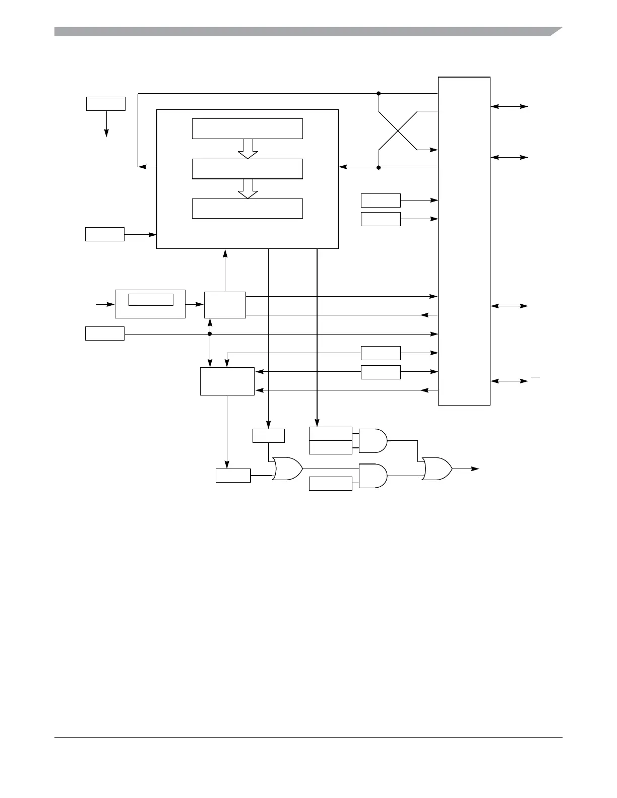
Figure 15-3. SPI Module Block Diagram
15.1.5 SPI Baud Rate Generation
As shown in Figure 15-4, the clock source for the SPI baud rate generator is the bus clock. The three
prescale bits (SPPR2:SPPR1:SPPR0) choose a prescale divisor of 1, 2, 3, 4, 5, 6, 7, or 8. The three rate
select bits (SPR2:SPR1:SPR0) divide the output of the prescaler stage by 2, 4, 8, 16, 32, 64, 128, or 256
to get the internal SPI master mode bit-rate clock.
SPI SHIFT REGISTER
SHIFT
CLOCK
SHIFT
DIRECTION
Rx BUFFER
FULL
Tx BUFFER
EMPTY
SHIFT
OUT
SHIFT
IN
ENABLE
SPI SYSTEM
CLOCK
LOGIC
CLOCK GENERATOR
US RATE
CLOCK
MASTER/SLAVE
MODE SELECT
MODE FAULT
DETECTION
MASTER CLOCK
SLAVE CLOCK
SPI
INTERRUPT
REQUEST
M
S
MASTER/
SLAVE
MOSI
(MOMI)
MISO
(SISO)
SPSCK
SS
M
S
S
M
MODF
SPE
LSBFE
MSTR
SPRF
SPTEF
SPTIE
SPIE
MODFEN
SSOE
SPC0
BIDIROE
SPIBR
Tx BUFFER (WRITE SPIxD)
Rx BUFFER (READ SPIxD)