Chapter 4 Memory
MC9S08QE128 MCU Series Reference Manual, Rev. 2
70 Freescale Semiconductor
4.6.1 Features
Features of the flash memory include:
• Flash size
— MC9S08QE128: 131,072 bytes (256 pages of 512 bytes each)
— MC9S08QE96: 98,304 bytes (192 pages of 512 bytes each)
— MC9S08QE64: 65,536 bytes (128 pages of 512 bytes each)
• Single power supply program and erase
• Automated program and erase algorithm
• Fast program and erase operation
• Burst program command for faster flash array program times
• Up to 100,000 program/erase cycles at typical voltage and temperature
• Flexible protection scheme to prevent accidental program or erase
• Security feature to prevent unauthorized access to the flash and RAM
• Auto power-down for low-frequency read accesses
4.6.2 Register Descriptions
The flash module contains a set of 16 control and status registers. Detailed descriptions of each register bit
are provided in the following sections.
4.6.2.1 Flash Clock Divider Register (FCDIV)
The FCDIV register is used to control the length of timed events in program and erase algorithms executed
by the flash memory controller.
All bits in the FCDIV register are readable and writable with restrictions as determined by the value of
FDIVLD when writing to the FCDIV register (see Table 4-11).
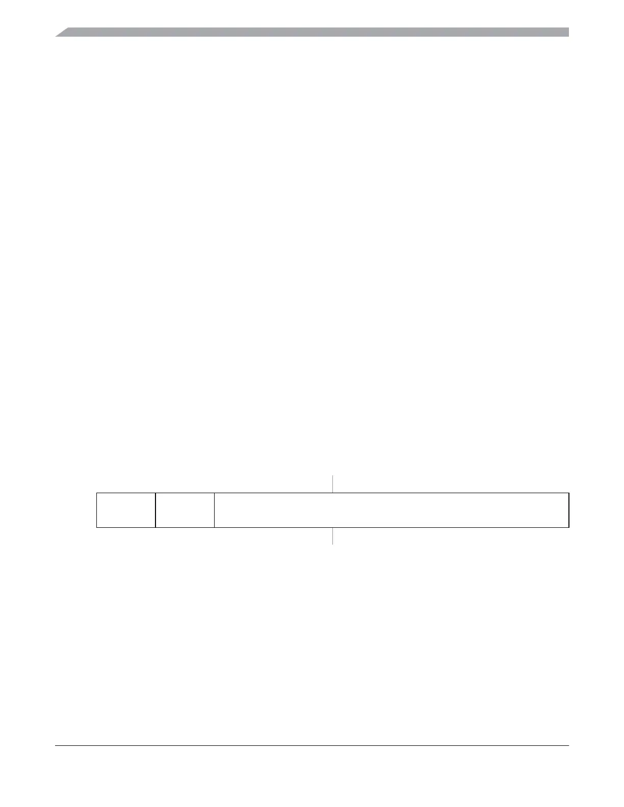
76543210
R
FDIVLD PRDIV8 FDIV
W
Reset 00000000
Figure 4-10. Flash Clock Divider Register (FCDIV)
 Loading...