CEM
3320
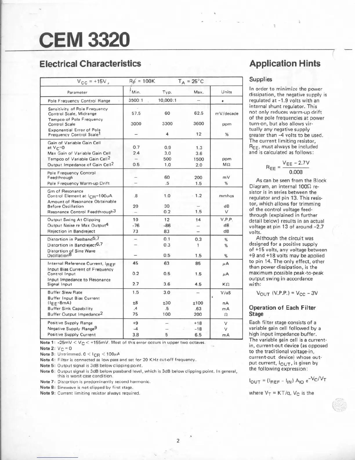
Electrical
Characteristics
Application
Hints
Pos~t~ve Supply
Range
+9
-
+18
V
Negat~ve Supply
~en~e~
4
-18
V
pns~t~ve Supply
Current
3.8
5
6.5
mA
Supplies
In
order to minimize
the
power
dissipation,
the
negative supply
is
regulated
at
-1
-9
volts with an
internal shunt regulator.
This
not
only reduces warm-up drift
of the pole frequencies
at
power
turn-on,
but
also atlows vir-
tually any
negative
supply
greater
than
-4
volts to
be
used.
The
current limiting resistor.
REE,
must
always
be
included
and
is
calculated
as
follows:
As
can
be
seen
from
the Block
Diagram,
an
internal
100a
re-
sistor is in series between
the
regulator
and
pin
13.
This resis-
tor, which
allows
far
trimming
of
the
control voltage feed-
through
(explained in further
detail below) results in an actual
voltage at
pin
13
of
around
-2.7
volts.
Although
the
circuit was
designed for
a
positive
supply
of
+I
5
volts,
any voiltage between
4-9
and
+I8
volts
may
be
applied
to
pin
14.
The
only
effect,
other
than
power
dissipation,
is
the
maximum possible peak-to-peak
output swing in accordance
with:
Operation
of
Each
Filter
Stage
Each filter
stage
consists
of
a
variable gain cell followed
by
a
high input
impedance
buffer.
Note
1:
-25mV
<
VC
<
+lSSrnV.
Most of
th~s
error
occurs In
upper
two
octaves.
The variable
gain
cell is
a
current-
Note
2:
VC
=
O
in, current-out device
(as
opposed
Note
3:
Untrimmed.
0
<
ICR
<
10OpA
to
the
traditional voltage-in,
Note
4:
F~lter
is
connected
as
low
pass
and
set
for
20
KHz
cut-off
frequency.
current-out
device)
whose out-
Note
5:
Output
s~gnal is
3dB
below clipping point.
put
current,
louT,
is
given
by
Note
6:
Output signal is
3dB
below passband
level,
which
is;
3dB
below clipping poinr. In general,
the following expression
:
this
IS
worst
case
cond~tion.
Note
7:
Distortron
15
predominantiy
second
harmonic.
Note
8:
Sinewave is not clipped
by
first
stage.
Note
9:
Current llmiting resistor always required.
where
Vr
=
KT/q,
Vc
is
the