voltage applied
to
pin
12.
AiO
is
the current gain
of
the
cell
'
at
VC
=
0
[Nominally
0.9).
and
.46Vcc
-
.65V
REF
=
IQOU*
As
the input to the variable
cell
is
a
farward
biased diode to
ground,
it
presents essentially
a
low
impedance
summing
node
at
a nominal
650rnV
above
ground.
The
required input
currents
may
therefore be
obtained with resistors term
minating
at this inpwt node.
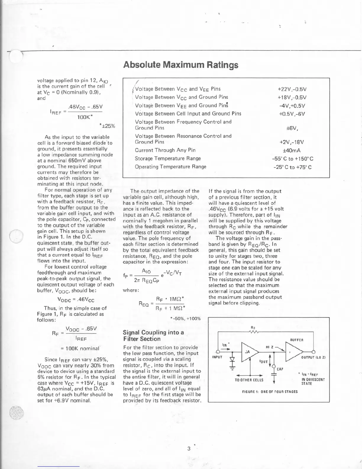
For normal
operation
of
any
filter
type.
each stage is
set
up
with
a
feedback resistor,
RF,
from
the buffer output
to
the
variable
gain
cell input, and with
the- pole capacitor,
Cp,
connected
to the
output of the variable
gain cell. This setup
is
shown
in Figure
1.
In the
D.C.
quiescent state, the buffer
out-
put will always adjust itself so
that
a
current
equal
to
lREF
flows
into
the
input.
For
lowest control voltage
feedthrough and maximum
peak-to-peak output signal, the
quiescent output voltage of each
buffer,
VODC,
should
be:
VoDc
=
.46Vcc
Thus, in
the
simple case
of
Figure
1,
RF
is calculated
as
follows:
=
100K
nominal
Since
IREF can vary
*25%,
VoDc
can
vary
nearly
30%
from
device
to device using
a
standard
5%
resistor for
RF.
In the typical
case where
VCC
=
+15V,
IREF
is
63pA
nominal, and the
D.C.
output
of
each
buffer should be
set
for
+6.9V
nominal.
Absolute
Maximum
Ratings
/
,'Voltage Between
Vcc
and
VE~
Pins
+22V,-0.5V
Voltage
Between
Vcc
and
Ground
Pins
+I
8V,-0.5V
Voltage Between
VEE
and
Ground
ping
-4V,+0.5V
Voltage Between Cell Input and Ground Pins
+0.5V,-6V
Voltage Between Frequency Control
and
Ground Pins
k6V,
Voltage Between Resonance Control and
Ground
Pins
+2V,-18V
Current Through
Any
Pin
f
40mA
Storage
Temperature Range
-55°C
to
+150"C
Operating Temperature Range
-25"
C
to
+75"
C
The output impedance of the
variable
gain
cell, although high,
has
a finite value. This imped-
ance
is
reflected
back
to the
input
as
an
b.C,
resistance
of
nominally
1
rnegohrn in parallel
with
the
feedback resistor.
RF
,
regard less of control voltage
value.
The
pole
frequency
of
each
filter section is determined
by
the
Total
equivalent feedback
resistance.
REa,
and the pole
capacitor in the expression:
where:
Signal
Coupling
into
a
F
ilter
Section
For the
filter
section
to provide
the
low
pass
function,
the
input
signal is coupled via
a
scaling
resistor,
Rc,
~nto the input.
Sf
the signal is the external input
to
the entire filter,
it
will in general
have
a
D.C.
quiescent voltage
level
of
zero,
and
all of l
l~
equal
to
IqEF for the first stage wil[
be
prov~ded
by
its
feedback
resistor.
If the signal
is
from
the output
of
a
previous
filter section,
it
will
have
a
quiescent level of
.46Vcc
(6.9
volts for
a
+I5
volt
supply}. Therefore, part
of
ll~
will be supplied
by
this voltage
through
RC
while the remainder
will
be
sourced
through
RF.
The voltage gain in the pass-
band
is
given
by
REQ/RC.
In
general, this gain should
be
set
to unity
far
stages
two,
three
and four. The input resistor to
stage
one
can
be
scaled
for any
size
of
the
external input signal.
The
resistance value should
be
selected
so
that
the
maximum
external input signal produces
the
maximum passband
output
signal before clipping.
"
111
=
IREF
IN
QUIESCERT
FIGURE
1
ONE
aF
FOURSTAGES