To
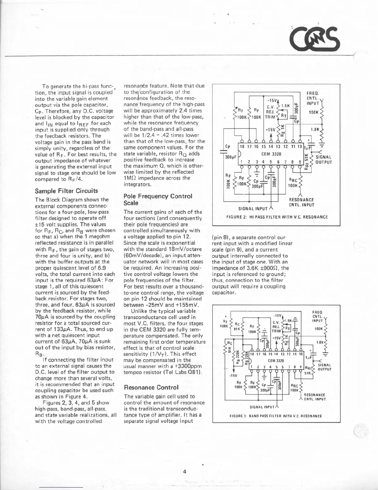
generate the
hi-pass
func-l
tion, the input signal
is
coupled
into
the
variable gain element
output via the pole capacitor,
Cp,
Therefore,
any
5.C.
voltage
level
is
blacked
by
the capacitor
and
IIN equal to
lREF
for each
input
is
supplied only through
The
feedback resistors. The
voltage gain in
the
pass
band
is
simply unity, regardless of the
value of
R
F.
For
best resu Its, the
output impedance of whatever
is generating
the
external
input
signal to stage one should
be
low
compared
to
R
F
14.
Sample
Filter Circuits
The Block Diagram shows the
extelrnal components connec-
tions for a four-pole, law-pass
filter designed to operate off
*I
5
volt supplies. The values
for
RF, RC,
and
RB
were chosen
so
that
a)
when the
1
megohm
reflected resistance is in parallel
with
RF,
the gain of stages
two,
three
and four
is
unity,
and
b)
with
the
buffer outputs
at
the
proper quiescent
lever of
6.9
volts, the total current
into
each
input is
the
required
63fiA:
For
stage
1,
afl
of
this
quiescent
current is sourced
by
the
feed-
back resistor.
For
stages two,
three, and four,
63pA
is sourced
by
the feedback resistor, while
70pA
is
sourced
by
the coupling
resistor for a total sourced cur-
rent
of
133pA.
Thus,
to
end up
with
a
net quiescent input
current
of
63pA.
70pA
is
sunk
out
of
the input
by
bias resistor,
Rs.
If connecting the filter input
to an exzernal signal causes
the
D.C.
level
of
the filter output
to
change more
than
several volts,
it is recommended that an input
coupling capacitor be
used such
as shown in Figure
4.
Figures
2.
3,
4,
and 5 show
high-pass, band-pass. all-pass,
and
state
variable realizations, all
with
the
voltage controlted
resonake feature. Note that
due
to
the,lconfiguration of the
resonince
feedback,
the
reso-
nance
frequency
of the high-pass
w~ll be approximately
2.4
times
higher than that
of
the
low-pass.
while
the
resonance frequency
of the band-pass and all-pass
will be
f
/2.4
=
-42
times lower
than that of the low-pass, for the
same component
values.
For
the
state variable, resistor
Ra
adds
positive feedback to increase
the maximum
0,
which is other-
wise limited by the reflected
1
MS1
impedance across the
integrators.
Pole
Frequency
Control
Scale
The
current
gains
of
each
of
the
four
sections
(and
consequently
their pole frequencies) are
controlled simultaneously with
a
voltage applied to pin
12.
Since
the
scale is exponential
with
the standard 18mV/octave
{GOrnV/decade), an input atten-
uator network will
in
most
cases
be
required. An increasing posi-
tive control voltage lowers the
pole frequencies
of
the filter.
For best results over
a
thousand-
to-one control range.
the
voltage
an
pin
I2
should
be
maintained
between
-25mV
and
+155mV.
Unlike the typical variable
transconductance
cell
used
in
most V.C. filters, the
four
stages
in the
CEM
3320
are
fully tem-
perature compensated.
The
only
remaining first order temperature
effect is that
of
control scale
sensitivity
(l/VT).
This
effect
may
be compensated
in
the
usual manner with
a
+3300ppm
tempco resistor ITel
Labs
081
11.
Resonance
Control
The variable gain cell used
to
control the
amount
of resonance
is
the traditional transconduc-
tance type of amplifier. It
has
a
separate
signal voltage input
L
f
FIGURE
2.
HE
PASS
FILTER WITH
V
C
AESOIYRNCE
(pin
8),
a
separate control cur-
rent input with
a
modified linear
scale (pin
9),
and
a
current
output internally connected to
the
input of szage
one.
With an
impedance
of 3.6K
f9005l,
the
input
is
referenced
to
ground;
thus, connection to the filter
output will require
a
coupling
caeacitor.