ICR
(PA)
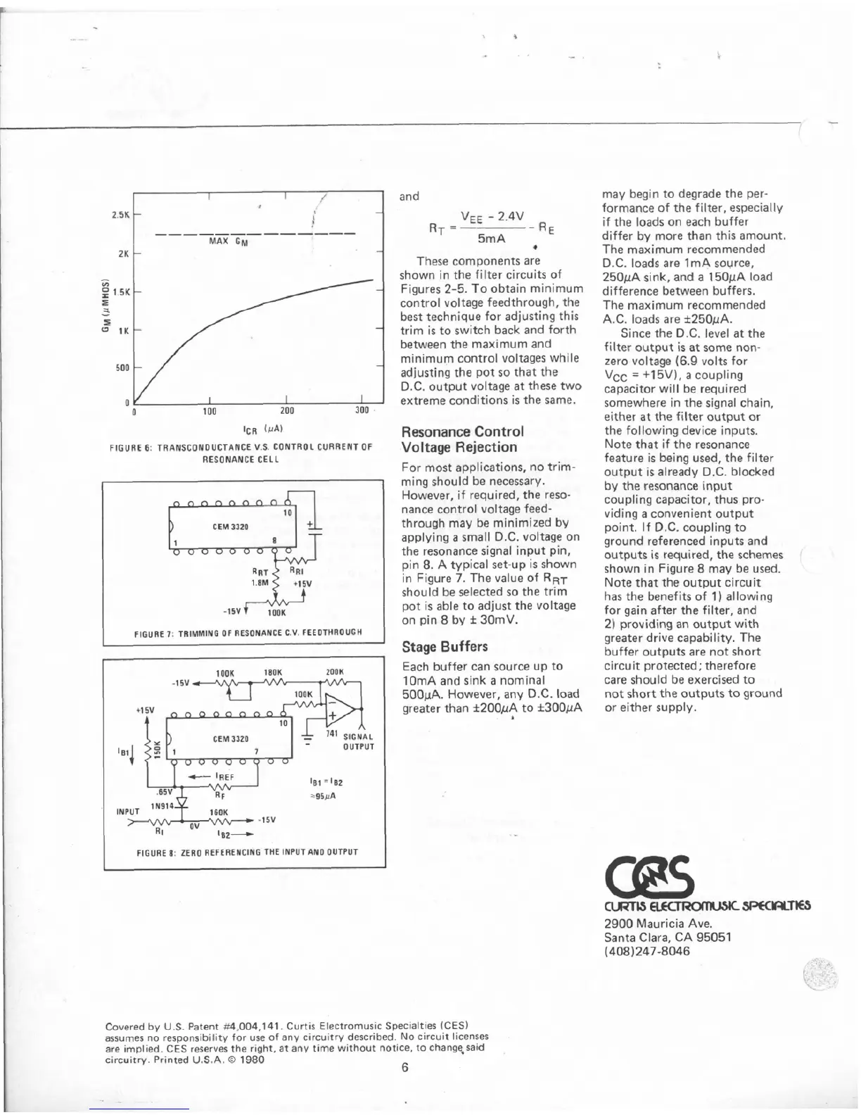
FIGURE
6:
TRANSCONDUCTANCE
V.S.
CONTROL
CUBAEnlT
OF
RESONANCE CELL
200K
FIGURE
8:
ZERO
REFERENCING
THE
INPUT
AN0
OUTPUT
and
These components are
shown in the filter circuits of
Figures
2-5.
To
obtain minimum
control
voltage feedthrough,
the
best technique for adjusting this
trim
is to switch
back
and forth
between the
maximum
and
minimum control voltages while
adjusting
the
pot so
that
the
D.C.
output voltage at
these
two
extreme conditions is the
same.
Resonance
Control
Voltage
Rejection
For most applications, no trim-
ming should
be
necessary.
However,
if
required, the reso-
nance control
voltage
feed-
through
may
be
minimized by
applying
a
small
D.C.
voltage on
the resonance signal input
pin,
pin
8.
d
typical set-up is shown
in Figure
7.
The value
of
RRT
should
be
selected
so
the trim
pot
is
able to adjust
the
voltage
on pin
8
by
f
3QmV.
Stage
Buffers
may
begin
to
degrade the per-
formance
of
the
filter,
especially
if the loads on
each
buffer
differ
by
more than this amount.
The
maximum recommended
D.C.
loads are
tmA
source.
251)uA
sink,
and
a
150yA
load
difference between buffers.
The
maximum recommended
A.C.
loads
are
f250pA.
Since the
D.C.
level
at
the
filter
output
is
at
some non-
zero voltage
(6.9
volts
for
Vcc
=
+15V),
a
coupling
capacitor
will
be
required
somewhere in the signal
chain,
either
at
the
filter
output
or
the
following device inputs.
Note
that if
the
resonance
feature
is
being
used,
the filter
output
is
already
D.C.
blocked
by
the
resonance
input
coupling capacitor, thus pro-
viding
a
convenient output
point. If
D.C.
coupling ta
ground
referenced
inputs and
outputs
is
required,
the
schemes
shown in Figure
8
may
be
used.
Note that the output circuit
has the benefits of
1
)
allowing
far
gain
after
the
filter,
and
2)
providing
an
output
with
greater
drive
capability. The
buffer
outputs are not short
Each
buffer
can source up to
circuit protected; therefore
lOmA
and
sink
a
nominal
care
should
be exercised to
SOOpA.
However, any
D.C.
laad
not short the outputs
to
ground
greater than
+200pA
to
+300uA
or
either supply.
h
2900
Mauricia
Ave.
Santa Clara,
CA
95051
(408)247-8046
Covered
by
U.S.
Patent
g4,004,141.
Curtis
Electromusic
Specialties
(CESI
assumes
no
respons~btl~ty
for use
of
any
c~rcu~tv
descrrbed.
No
clrcult lrcenses
are
impl~ed.
CES
reserves
the
right.
at
any
rime
without
notice,
to
change,sa!d
circu~try.
Printed
W.S.A.
C3
1980
6