lnput
and
Output
Waveforms
/
I
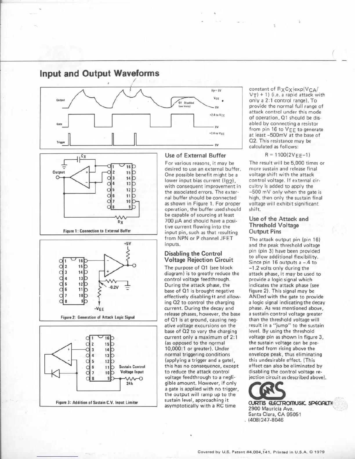
Use
of
External
Buffer
For various reasons,
it
may
be
desired to use
an
external buffer.
One possible
benefir might
be
a
lower input
bias
current
(152).
with consequent improvement in
the associated errors.
The
exter-
nal buffer should
be
connected
as
shown in Figure
I.
For proper
operation, the
buffer
used should
Figurn
3:
Addition
of
Susmin
C.Y.
lnput
Limiter
AX
Figure
I:
Connection
to
Extuna!
Buffer
constant of
RxCx(exp(Yc~/
VT}
+
1)
(i.e.
a
rapid attack with
only
a
2:l
control range).
To
provide the normal full range of
attack control under this mode
of
operation,
Q1
should
be
dis-
abled
by
connecting
a
resistor
from pin
16
to
VEE
to generate
at
least
-500mY
at
the
bass
of
Q2. This resistance
may
be
calculated
as
fellows:
R
=
1100(2V~~-1)
The result will
be
5.000
times
or
more sustain and release Final
voltage shift with the
attack
control voltage, If external clr-
cuitry
is
added
to apply
the
-500
mV
only
when
the gate is
high,
then only the sustain final
voltage will exhibit significant
sh~ft.
be capable
of
sourcing
at
least
700
PA
and should
have
a
posi-
tive current flowing into
the
input pin, such as that resulting
Use
of
the
Attack
and
Threshold
Voltage
Output
Pins
The attack output pin (pin
16.1
and the ~eak threshold
voltaae
from
NPN
or
P
channel
JFET
inputs.
Disabling the
Control
pin (pin.31
have
been provided
to allow additional flexibility.
Voltage
Rejection
Circuit
Since pin
16
outauts a
-.4
to
The purpose of
01
(see block
diagram) is to greatly reduce the
control voltage feedthrough.
During the attack
phase, the
base
of
Q1
is
brought negative
effectively disabling
it
and allow-
ing
Q2 to control the charging
current. During the
decay and
release phases, however, the
base
of
01
is at ground. causing neg-
ative voltage excursions on
the
base
of
Q2
to vary
the
charging
current
onfy
a
maximum of
2:1
(as
opposed
to
the normal
10,000:
1
or
greater). Under
normal triggering conditions
(applying
a
trigger
and
a
gate),
this has
no
consequence, except
to reduce the attack control
voltage feedthrough to
a
negli-
gibre
amount. However,
if
only
a
gate
is
applied with
no
trigger.
the output will ramp
up
to
the
sustain level, approaching
it
asymptotically with
a
RC
time
-1.2
volts only during the
attack
phase,
it
may
be
used to
provide
a
logic signal which
indicates the attack phase
(see
figure 2). This signa'l may be
ANDed with the gate to provide
a
logic signal indicating the decay
phase.
As
was
mentioned
above,
a
sustain control voltage
greater
than the threshold voltage will
result in
a
"jump"
to
the sustain
level.
By
using the threshold
voltage pin as
shown
in figure
3,
the sustain voltage can
be
pre-
vented from rising
above
the
envelope
peak.
thus eliminating
this undesirable effect.
(This
effect can also
be
eliminated
by
disabling the control voltage re-
jection circuit as described above).
cum-Keh--Tlc
2900
Maurrcia
Ave.
Santa Clara,
CA
95051
.
(408)247-8046
a
Covered
by
U.S.
patent
#a,ow,i'4~.
Pranted
in
U.S.A.
B
1979