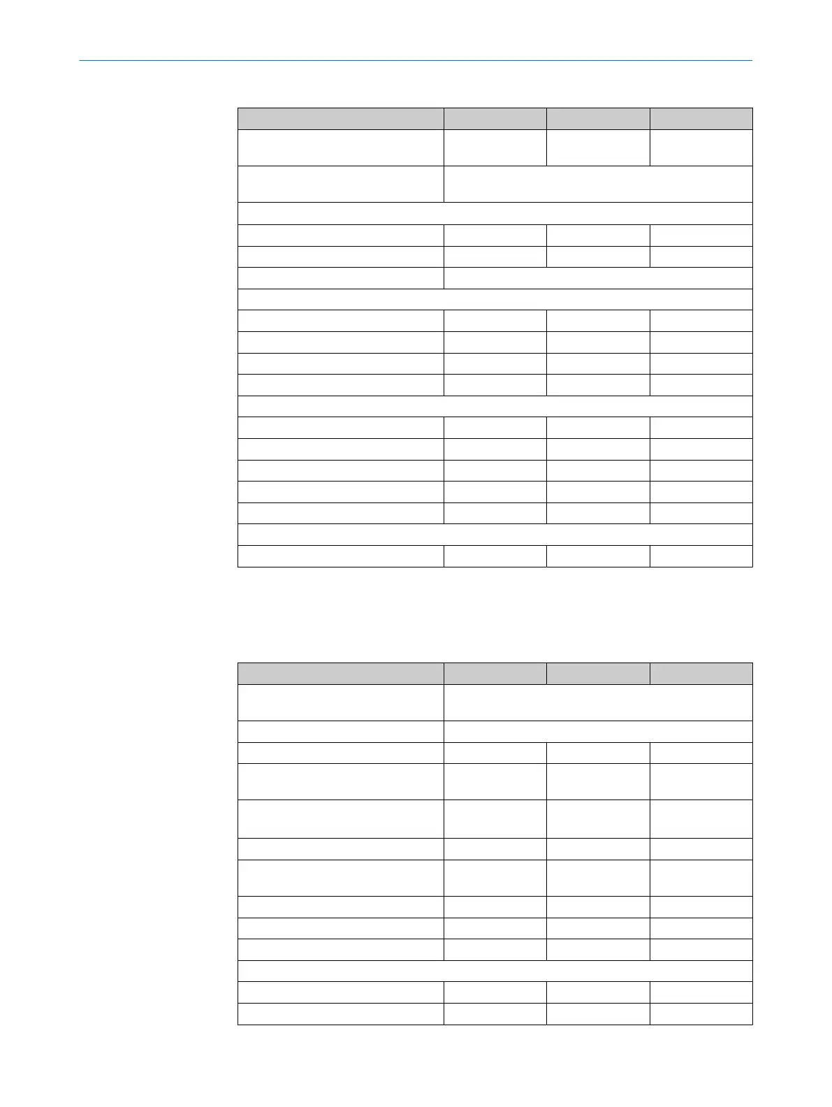
Table 29: Technical data for sender
Minimum Typical Maximum
Wavelength of sender Near-infrared
(NIR
), invisible
Weight Depending on the protective field height, see "Table of
weights", page 83
Laser alignment aid
Wavelength 650 nm (red)
Average output power 390 µW
Laser class 1
Laser alignment aid switch input (In1)
Input voltage HIGH (active) 13 V 24 V 30 V
Input current HIGH 2 mA 5 mA 7 mA
Input voltage LOW (deactivated) -3 V 0 V 3 V
Input current LOW -0.1 mA 0 mA 0.5 mA
Laser alignment aid pushbutton input (In2)
Input voltage HIGH (active) 13 V 24 V 30 V
Input current HIGH 2 mA 5 mA 7 mA
Input voltage LOW (deactivated) -3 V 0 V 3 V
Input current LOW -0.1 mA 0 mA 0.5 mA
Control switch actuation time 50 ms
Permissible cable resistance
1)
Supply cable 2.5 Ω
1)
Limit the individual conductor resistance to the specified values to ensure that the light curtain functions
cor
rectly. (Also observe IEC 60204-1.)
The specified values apply to the total resistance of each wire including contact and connector resistan‐
ces.
Table 30: Technical data for receiver
Minimum Typical Maximum
Output signal switching devices
(OS
SDs)
2 PNP semiconductors, short-circuit protected
1)
, cross-
circuit monitored
Response time "Response time", page 82
Duration of OFF state 100 ms
Switch-on delay 3 × response
t
ime
ON state, switching voltage HIGH
(U
rms
)
2)
U
V
– 2.25 V 24 V U
V
OFF state, switching voltage LOW
2)
3)
0 V 0 V 2.0 V
Current-carrying capacity of the
O
SSDs
500 mA each
Leakage current of the OSSDs 2 mA each
Load capacity 2.2 µF
Load inductance 2.2 H
Test pulse data
4)
Test pulse width 150 µs 300 µs
Test pulse rate 3 s
-1
5 s
-1
10 s
-1
13 TECHNICAL DATA
80
O P E R A T I N G I N S T R U C T I O N S | deTec4 8027140/2021-11-04 | SICK
Subject to change without notice
 Loading...