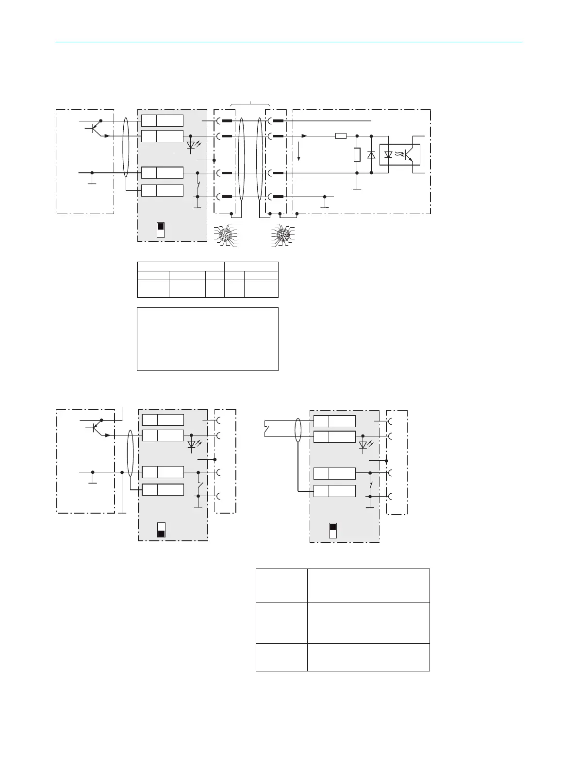
Wire switching inputs “Sensor 1 ... 2” of the CLV69x in the CDB650-204 connection module
CLV69xCDB650-204
PNP sensor
U
V
U
V
U
V
GND
SensGND
3.32K
6.64K
Sensor Z
U
e
Y
99
a) Sensor supplied via CDB650-204
2
2)
1
Y
2
1
12
SGND
6
Shield
11
U
IN
*
X Name
Out
U
IN
*
GND
S3
e.g. photoelectric
sensor
ON
OFF
S3: SGND-GND
Specifications of the switching inputs “Sensor 1 and 2”
Logic
Properties
Electrical values
Shield
GND
.
.
.
U
e
= max. 32V
17
16
10
11
12
15
14
6
5
4
13
7
8
9
1
2
3
17
16
10
11
12
15
14
6
5
4
13
7
8
9
1
2
3
b) Sensor connected volt-free and supplied externally
CDB650-204
PNP sensor
U
V
GND
12
SGND
6
Shield
11 U
IN
*
X
Out
U
IN
*
GND
S3
e.g. photoelectric
sensor
ON
OFF
S3: SGND-GND
U
V ext
Shield
Name
d) Diagram: switch connected volt-free and
supplied externally
Connection of the switch as under b)
c) Switch supplied via CDB650-204
U
IN
*
CDB650-204
12 SGND
6 Shield
11
U
IN
*
X
GND
S3
ON
OFF
S3: SGND-GND
Shield
Name
SensGND
GND
M12,
17-pin,
A-coded
Switch S3: SGND-GND
ON: GND of the switching inputs connected
with GND of the CDB650-204/CLV69x.
OFF: Sensors on switching inputs of the
CDB650-204/CLV69x connected volt-free.
Reference potential valid for all switching inputs
“SENS/IN 1 ... 2” and optionally “EXT. IN1 and 2”
CDB650-204 CLV69x
Terminal X
10
13
Name
SENS/IN 1
SENS/IN 2
Pin Y
10
15
Pin Y
10
15
Sensor Z
Sensor 1
Sensor 2
Functional allocation for switching inputs
via SOPAS-ET configuration software.
For CLV69x-xxx0 (without heating):
no. 6052286 (2m)
no. 6051194 (3m)
no. 6051195 (5m)
For CLV69x-xxx1 (with heating):
no. 6053230 (2m)
no. 6053231 (3m)
no. 6053232 (5m)
1) Dependent on type
Connection cable 1:1
1)
2) Pin 2 in the CLV69x-xxx1
(with heating) not
connected
Current to input starts the assigned
function, e.g. start read cycle.
(Default CLV69x: logic active high,
debounce 10mm)
– Opto-decoupled, reverse-polarity
protected
– Can be wired with PNP output of a sensor
– SensGND is the shared, insulated
reference potential for all switching inputs
Low: U
e
≤ 2V; I
e
≤ 0.3mA
High: 6V ≤ U
e
≤ 32V;
0.7mA ≤ I
e
≤ 5mA