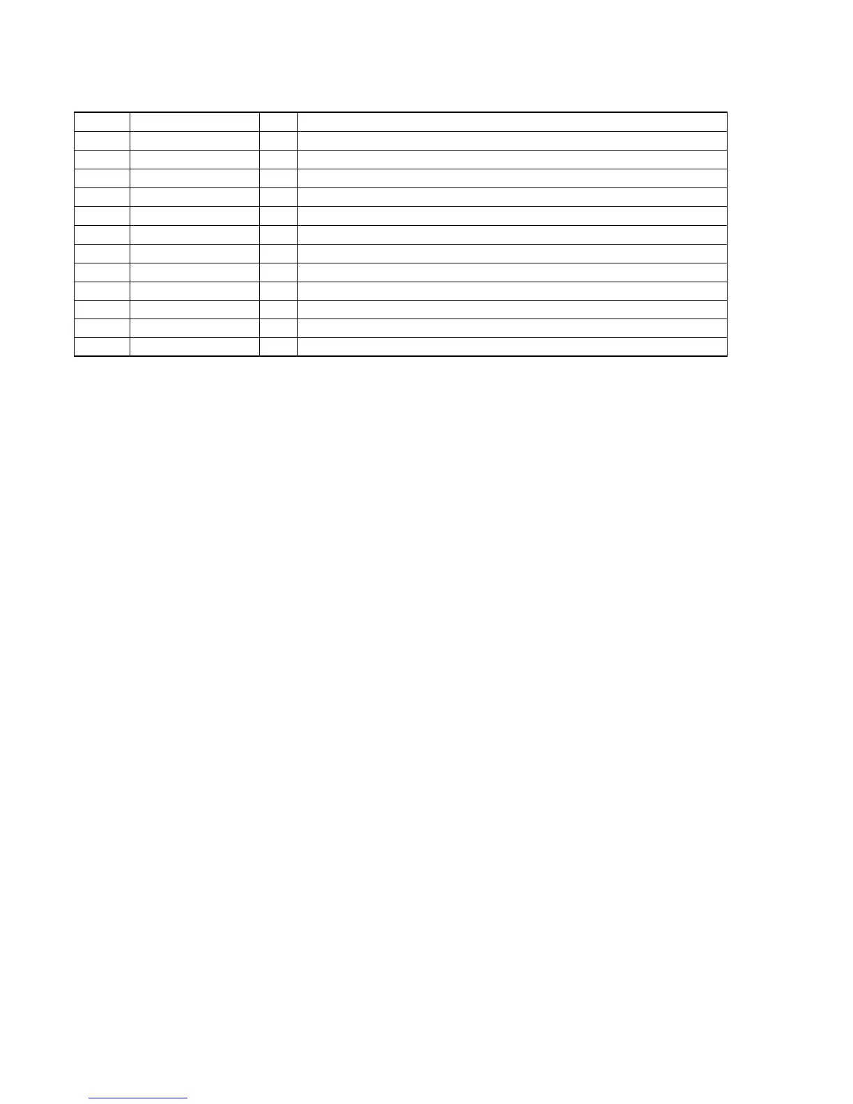
48
CDP-M400CS
Pin No. Pin Name I/O Description
53 PI5/DATA I General purpose input/SUBQ interface data input (fixed at “L”)
54 TSTIN/SFSY I Terminal for test/SUBQ interface frame sync input (fixed at “L”)
55 FI2/SBSY I Flag signal input 2/SUBQ interface block sync input (fixed at “L”)
56 VSSP — Ground for VCO circuit
57 PDO O PLL phase error detection signal output
58 VCOI I VCO control voltage input
59 VDDP — Power supply (2.5V) for VCO circuit
60 CKO O External clock output
61 VDDX — Power supply (2.5V) for oscillation circuit
62 XI I Resonator terminal (input)
63 XO O Resonator terminal (output)
64 VSSX — Ground for oscillation circuit