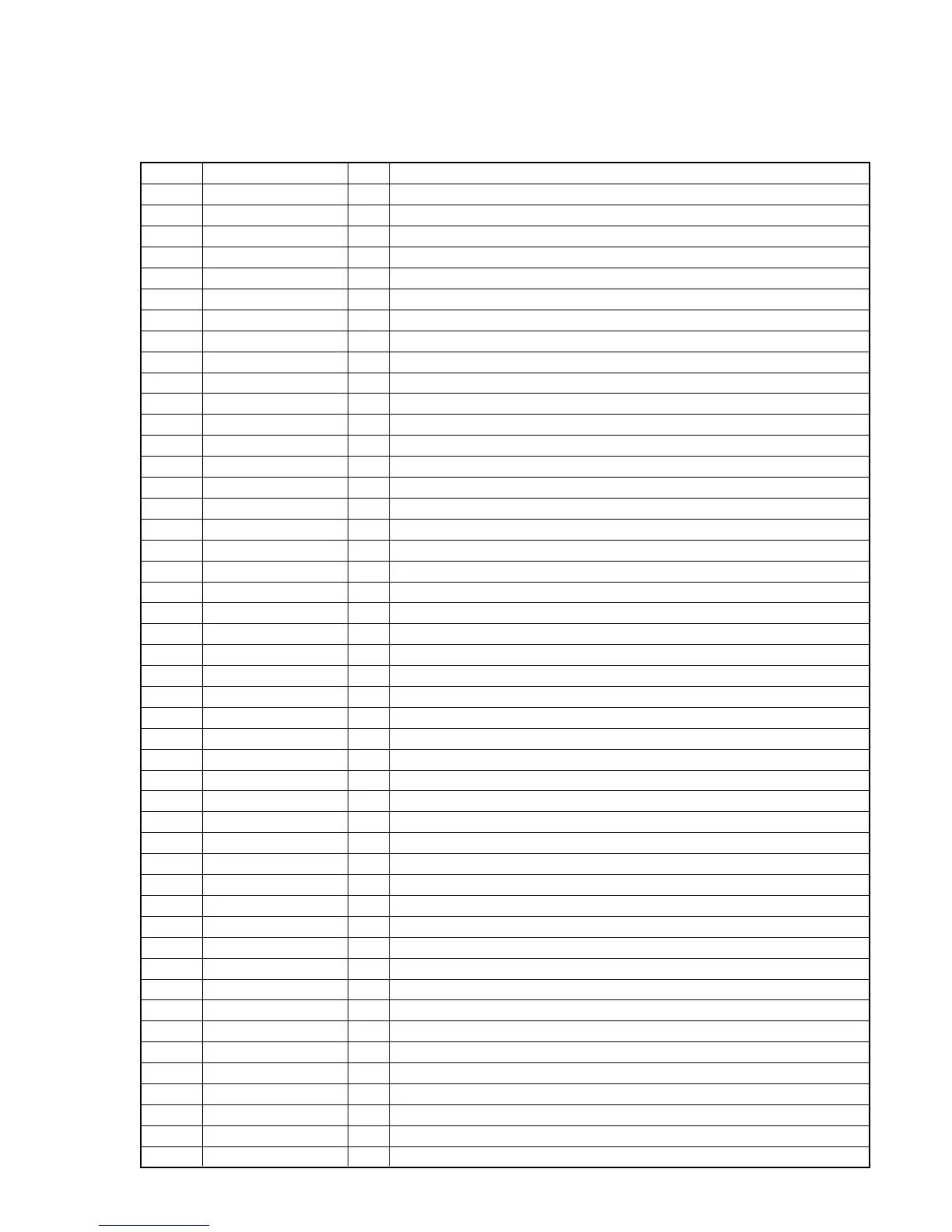
49
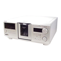
CDP-M400CS
MAIN BOARD IC501 µPD703030BYGF-M13-3BA (SYSTEM CONTROL)
Pin No. Pin Name I/O Description
1 FLDATA O Data signal output to the fluorescent indicator drivers amd LED driver
2 FLCLK O Clock signal output to the fluorescent indicator drivers and LED driver
3 LEDLAT O Latch signal output to the LED driver
4DATAOData output to the DSP
5 CLK O Clock signal output to the DSP
6 SENS I SENS signal input from the DSP
7 MP3RST O Reset signal output to the IC104
8 FLRST O Reset signal output to the the fluorescent indicator driver amd LED driver
9 EVDD — Power supply (I/O port)
10 EVSS — Ground (I/O port)
11 PWM1 O PWM1 signal output
12 PWM2 O PWM2 signal output
13 RMIN I Data input from the remote control receiver
14 BUSOUT O CONTROL A1 signal output
15 SUBQ I CD SUBQ signal input from the DSP
16 BUSIN I CONTROL A1 signal input
17 SQCK O CD SUBQ clock signal output to the DSP
18 AMUTE O Muting signal output to the IC104
19 PWM3 O PWM3 signal output
20 XLT O Latch signal output to the DSP
21 IC/VPP — Connected to ground
22 TBLR O Table motor control signal output (clockewise)
23 TBLL O Table motor control signal output (counterclockewise)
24 LDOUT O Loading motor control signal output (out)
25 LODIN O Loading motor control signal output (in)
26 DOORIN O Door motor control signal output (close)
27 DOOROUT O Door motor control signal output (open)
28 ICSW O Power supply to the peripheral ICs
29 SMUTE O 2nd audio input muting signal output
30 SBLED O Sandby LED control signal output
31 LED O Inside illumination LED control signal output
32 DSENSOUT O Disc sensor readout result signal output
33 H-HOUT O Or signal of TSENS1/TSENS2 output
34 RESET I System reset input
35 XT1 I Sub clock input
36 XT2 O Sub clock output
37 REGC – Capacitor connection terminal for regulator output stabilizing
38 X2 O Main system clock output
39 X1 I Main system clock input
40 VSS — Ground
41 VDD — Power supply
42 CLKOUT O Clock output (open)
43 FLT2 O Fluorescent indicator driver (IC704) latch signal output
44 FLT1 O Fluorescent indicator driver (IC701) latch signal output
45 KBCO O Keyboard clock output
46 XRST O Peripheral ICs reset signal output
47 CE O SRAM chip enable signal output