50
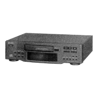
CDP-M400CS
Pin No. Pin Name I/O Description
48 WE O SRAM write enable signal output
49 A4 O SRAM address signal output
50 D0 I/O SRAM data bus
51 to 57 D1 to D7 I/O SRAM data bus
58 BVDD — Power supply (I/O port)
59 BVSS — Ground (I/O port)
60, 61 A13, A14 O SRAM address signal output
62 A0 O SRAM address signal output
63 to 70 A5 to A12 O SRAM address signal output
71 to 73 A1 to A3 O SRAM address signal output
74 AVDD — Power supply (A/D converter)
75 AVSS — Ground (A/D converter)
76 AVREF — Reference voltage for A/D converter
77 ADJ I selector (ADJ/AFADJ)
78 DOORSW I Door switch signal input (A/D)
79 LDSW I Loading switch signal input (A/D)
80 KEY0 I Key data signal input (A/D)
81 DJOG2 I Jog signal input
82 TJOG2 I AMS jog signal input
83 TJOG1 I AMS jog signal input
84 DJOG1 I Jog signal input
85 KBDI I Keyboard data input
86 DSENS I Disc sensor signal input
87 TSENS1 I Table sensor signal input
88 TSENS3 I Table sensor signal input
89 KBDO O Keyboard data output
90 POWER I POWER key signal input
91 TSENS2 I Table sensor signal input
92 TSENS4 I Table sensor signal input
93 KBCI I Keyboard clock input
94 ACIN I AC power detection signal input
95 SCOR I Sync signal input from the DSP
96 MP3REQ I MP3 request signal input from the IC104
97 SDA/SI0 I/O MP3 IIC data input or output
98 RFSW/SO0 O Mode selection signal output to the RF amplifier (IC103)
99 SCL/SCK0 O MP3 clock output to the IC104
100 FLDATA_I I Data input from the fluorescent indicator driver