47
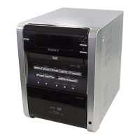
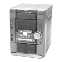
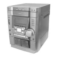
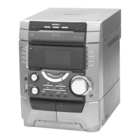
HCD-DV2D
MPEG BOARD UD705 ZR36748 (VIDEO DAC ENCODER)
Pin No. Pin Name I/O Description
1 VDDP — Power supply terminal (+3.3V)
2 DUPRD — Not used
3 BOOTSEL2 — Not used
4 GPCI014 I LSI RST signal input from the AV decoder
5 GPCI013 — Not used
6 GPCI012 — Not used
7 SSCRRO/CPC1011 I Chip enable signal input from the system controller
8 SSCRRO/CPC1010 I Clock signal input from the system controller
9 to 14 ATDD5 to 10 I DVD (RF) signal input from the AV decoder
15 GNDP — Ground terminal
16 ATDD4 I DVD (RF) signal input from the AV decoder
17 VDDP — Power supply terminal (+3.3V)
18 ATDD11 I DVD (RF) signal input from the AV decoder
19 ATDD3 I DRFO signal input from the AV decoder
20 ATDD12 I DACK signal input from the AV decoder
21 ATDD2 I DFFR signal input from the AV decoder
22 ATDD13 I DBGN signal input from the AV decoder
23 ATDD1 I DCLK signal input from the AV decoder
24 ATDD14 — Not used
25 ATDD0 I DMUTE signal input
26 ATDD15 O DVD tray open signal output
27 ATIOW O DVD tray close signal output
28 VDDC — Power supply terminal (+1.8V)
29 ATIOR O LMTSW signal output from the AV decoder
30 GNDP — Ground terminal
31 ATIORD I RDY signal input
32 ATIOFFRO — Not used
33 GNDP — Ground terminal
34 ATDA2 O RF servo gain up signal output
35 VDDP — Power supply terminal (+3.3V)
36 ATDA1 I C2F signal input from the AV decoder
37 ATDA0 I LRCK signal input from the AV decoder
38 ATCS1 I BCK signal input from the AV decoder
39 ATCS0 I CD DATA signal input from the AV decoder
40 BOOTSEL1 — Not used
41 GPCI01 I INTDET signal input from the AV decoder
42 SSCSRO I Not used in this set. Fixed at (“L”).
43 GPC103 I WRO signal input from the AV decoder
44 GCP104 — Not used
45 GCP105 O Serial data output to the audio DAC
46 GCP106 O Serial data clock output to the audio DAC
47 GCP107 I SPDFG signal input
48 VDDP — Power supply terminal (+3.3V)
49 SSCRXD/GPC108 I Data signal input from the system controller
50 GNDP — Ground terminal
51 SSCRXD/GPC109 I Data signal input from the system controller
52 VDDP — Power supply terminal (+3.3V)
53 to 55 RAMADD0 to 3 O Address bus to the D-RAM