48
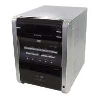
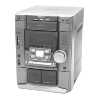
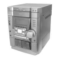
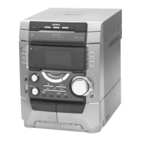
HCD-DV2D
Pin No. Pin Name I/O Description
56 GNDP — Ground terminal
57 to 60 RAMADD4 to 7 O Address bus to the D-RAM
61 VDDP — Power supply terminal (+3.3V)
62 to 64 RAMADD8 to 11 O Address bus to the D-RAM
65 GNDP — Ground terminal
66 RAMBA1 O Chip select signal output to the D-RAM
67 RAMADD2 O Address bus to the D-RAM
68 RAMBA0 O Address bus to the D-RAM
69 VDDP — Power supply terminal (+3.3V)
70 RAMADD11 — Not used
71 RAMCS — Not used
72 RAMRAS O D-RAM Low address strobe signal output
73 GNDP — Ground terminal
74 RAMCAS O D-RAM column address strobe signal output
75 RAMWE O D-RAM write enable signal output
76 RADOM O D-RAM data signal output
77 VDDP — Power supply terminal (+3.3V)
78 PCLK O D-RAM clock output
79 GNDP — Ground terminal
80 RAMDAT8 I/O Databus to the D-RAM
81 GNDC — Not used
82 RAMDAT7 I/O Databus to the D-RAM
83 VDDC — Power supply terminal (+1.8V)
84 RAMDAT9 I/O Data bus to the D-RAM
85 VDDP — Power supply terminal (+3.3V)
86 RAMDAT6 I/O Databus to the D-RAM
87 RAMDAT10 I/O Databus to the D-RAM
88 GNDP — Ground terminal
89 RAMDAT5 I/O Databus to the D-RAM
90 RAMDAT11 I/O Databus to the D-RAM
91 VDDP — Power supply terminal (+3.3V)
92 RAMDAT4 I/O Databus to the D-RAM
93 RAMDAT12 I/O Databus to the D-RAM
94 GNDP — Ground terminal
95 RAMDAT3 I/O Databus to the D-RAM
96 RAMDAT13 I/O Databus to the D-RAM
97 VDDP — Power supply terminal (+3.3V)
98 RAMDAT2 I/O Databus to the D-RAM
99 RAMDAT14 I/O Databus to the D-RAM
100 GNDP — Ground terminal
101 RAMDAT1 I/O Databus to the D-RAM
102 RAMDAT15 I/O Databus to the D-RAM
103 VDDP — Power supply terminal (+3.3V)
104 RAMDAT0 I/O Databus to the D-RAM
105 MEMDA0 I/O Flash memory data bus
106 MEMDA12 I/O Flash memory data bus
107 MEMDA1 I/O Flash memory data bus
108 MEMDA13 I/O Flash memory data bus
109 MEMDA2 I/O Flash memory data bus