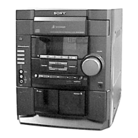
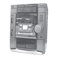
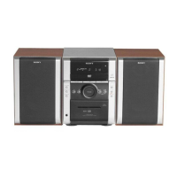
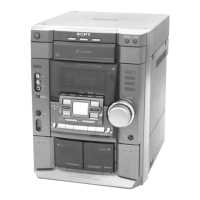
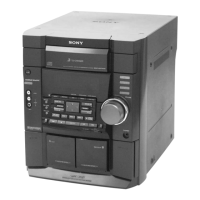
HCD-DX90
2525
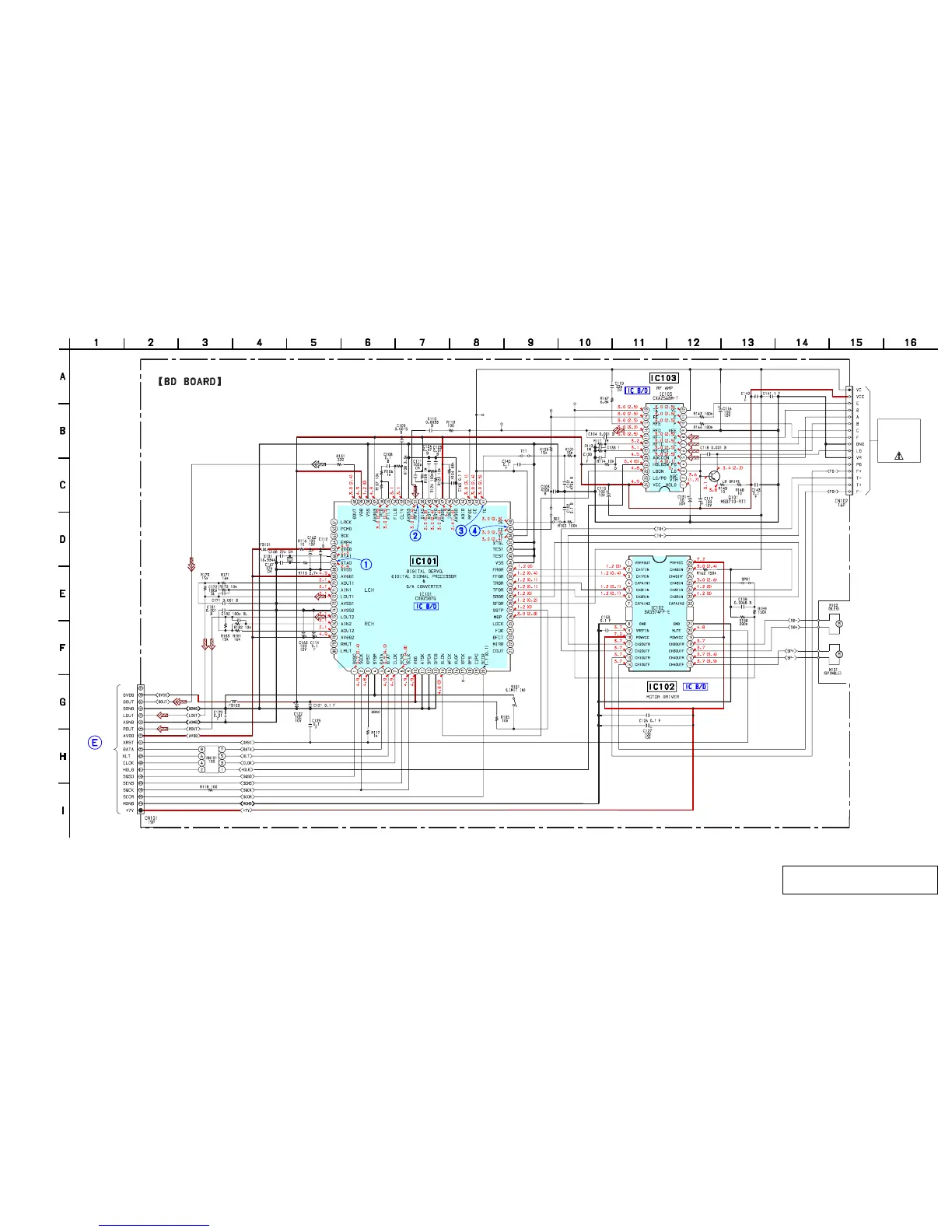
7-4. SCHEMATIC DIAGRAM – BD SECTION – • See page 21 for Wavefoms. • See page 42 for IC Block Diagrams.
OPTICAL
PICK-UP
BLOCK
(KSM-213DAP)
MAIN BOARD (3/3)
CN201
TP
(XPCK)
TP
(VC)
TP
(RFO)
TP
(FEO)
TP
(TEO)
TP
(AGCCON)
TP
(FE1)
(Page 29)
• Voltages and waveforms are dc with respect to ground
under no-signal conditions.
no mark : CD STOP
The components identified by mark 0 or dotted
line with mark 0 are critical for safety.
Replace only with part number specified.


 To Next Page