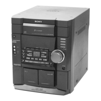
HCD-DX90
3131
MAIN BOARD (3/3)
CN902
MAIN BOARD (3/3)
CN901
TRANS BOARD
CN978
TRANS BOARD
CN977
TRANS BOARD
CN977
470
470
RBV-602
NO505
VH
VH
GND
VL
VL
0.001
0.001
STK-412-040
STK-412-040
1.5k
MTZJ-T-77-15B
0.22
0.22
82k
82k
1.5k
MTZJ-T-77-15B
0.22
0.22
82k
Q831
2SC1785
OVER HEAT
DETECT
R531
220
R532
560k
R533
47k
2SB1375
1
2
4
3
1
2
4
3
CN504
2P
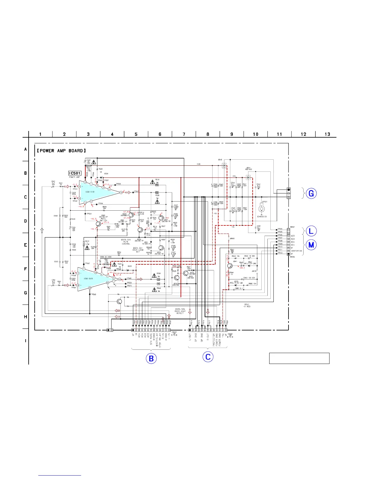
7-10. SCHEMATIC DIAGRAM – POWER AMP SECTION –
The components identified by mark 0 or dotted
line with mark 0 are critical for safety.
Replace only with part number specified.
(Page 29)
(Page 29)
(Page 39)
(Page 39)
(Page 39)
• Voltages and waveforms are dc with respect to ground
under no-signal conditions.
no mark : CD STOP


 To Next Page