HCD-GN1300D
HCD-GN1300D
3131
For Schematic Diagrams.
Note:
• All capacitors are in F unless otherwise noted. (p: pF)
50 V or less are not indicated except for electrolytics and
tantalums.
• All resistors are in and
1
/4 W or less unless otherwise
specifi ed.
• % : indicates torelance.
•
f
: internal component.
• 2 : nonfl ammable resistor.
• 5 : fusible resistor.
• C
: panel designation.
• A : B+ Line.
• B : B– Line.
• Voltages and waveforms are dc with respect to ground
under no-signal (detuned) conditions.
DMB16 and VIDEO boards
no mark : DVD PLAY
Other board
no mark : TUNER (FM/AM)
( ) : DVD PLAY
< > : TAPE PLAY
[ ] : TAPE REC
*
: Impossible to measure
• Voltages are taken with VOM (Input impedance 10 M).
Voltage variations may be noted due to normal production
tolerances.
• Waveforms are taken with a oscilloscope.
Voltage variations may be noted due to normal production
tolerances.
• Circled numbers refer to waveforms.
• Signal path.
F : AUDIO
e : TUNER
k : TAPE PLAY (DECK A)
d : TAPE PLAY (DECK B)
G : REC (DECK B)
J : CD PLAY
N : MIC
c : DVD PLAY
L : VIDEO
E : Y
a : CHROMA
r : COMPONENT VIDEO
q : R, G, B
• Abbreviation
E4 : African model
E15 : Iran model
EA : Saudi Arabia model
MY : Malaysia model
PH : Philippines model
SP : Singapore model
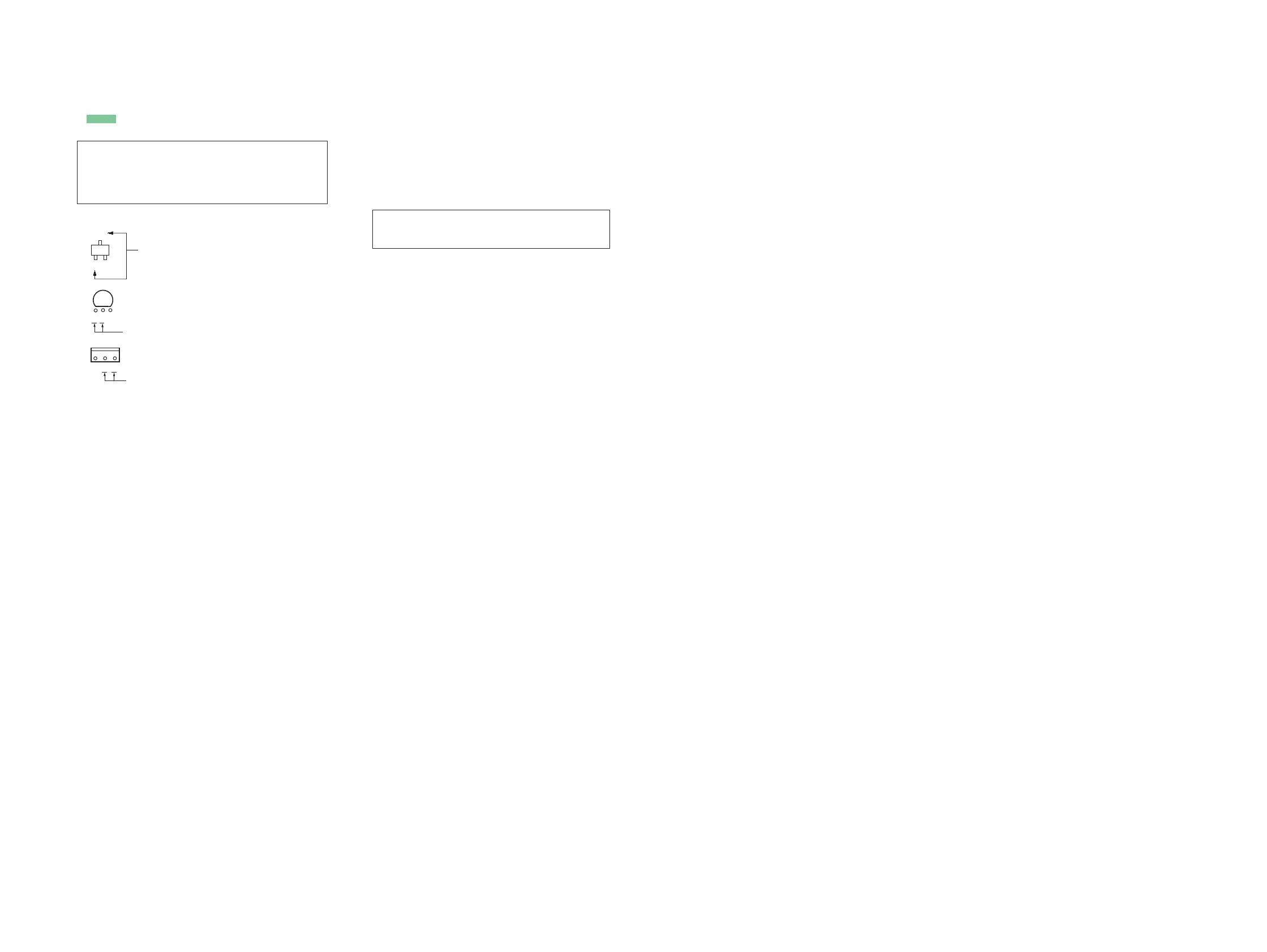
For Printed Wiring Boards.
Note:
• X : Parts extracted from the component side.
•
: Pattern from the side which enables seeing.
(The other layers' patterns are not indicated.)
• Indication of transistor.
• Abbreviation
E4 : African model
E15 : Iran model
EA : Saudi Arabia model
MY : Malaysia model
PH : Philippines model
SP : Singapore model
Caution:
Pattern face side:
(SIDE A)
Parts face side:
(SIDE B)
Parts on the pattern face side seen from
the pattern face are indicated.
Parts on the parts face side seen from
the parts face are indicated.
Note: The components identifi ed by mark 0 or dotted
line with mark 0 are critical for safety.
Replace only with part number specifi ed.
C
B
These are omitted.
E
Q
CEB
These are omitted.
These are omitted.
CBE
 Loading...