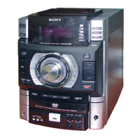
HCD-GN1300D
76
149 RA11 O DRAM address output bit 11
150 to 155 RA9 to RA4 O DRAM address output bit 9 to 4
156 DVDD3 – Power supply pin (+3.3 V) for internal digital circuitry
157 MUTE123 O Mute signal output for other motor drivers (SL, TRK, FCS)
158 MUTE O Mute signal output for spindle motor driver
159 DDC_DA I/O HDMI DDC line SDA
160 DVDD18 – Power supply pin (+1.8 V) for internal digital circuitry
161 DDC_CLK I/O HDMI DDC line CLK
162 HTPLG I Hot plug detection input
163 AGND3 – Analog ground pin for HDMI TX
164 EXT_RES I External resistor for HDMI TX
165, 166 AVDD3 – Analog power supply pin (+3.3 V) for HDMI TX
167 EXT_CAP I External capacitor for HDMI TX
168 AGND3 – Analog ground pin for HDMI TX
169 AGND18 – Analog ground pin for HDMI TX
170 TXCN O Negative TX CLK output (Not used in this set)
171 TXCP O Positive TX CLK output (Not used in this set)
172 AVDD18 – Analog power supply pin (+1.8 V) for HDMI TX
173 TX0N O Negative TX 0CH output (Not used in this set)
174 TX0P O Positive TX 0CH output (Not used in this set)
175 AGND18 – Analog ground pin for HDMI TX
176 TX1N O Negative TX 1CH output (Not used in this set)
177 TX1P O Positive TX 1CH output (Not used in this set)
178 AVDD18 – Analog power supply pin (+1.8 V) for HDMI TX
179 TX2N O Negative TX 2CH output (Not used in this set)
180 TX2P O Positive TX 2CH output (Not used in this set)
181 AGND18 – Analog ground pin for HDMI TX
182 R/Cr/Pr O Red or CR output
183 B/Cb/Pb O Blue or CB output
184 DACVSSA – Ground pin for video DAC circuitry
185 Y/G O Green or Y output
186 DACVDDA – Power supply pin (+3.3 V) for video DAC circuitry
187 CVBS O Analog composite output
188 DACVSSB – Ground pin for video DAC circuitry
189 C O Analog chroma output
190 DACVDDB – Power supply pin (+3.3 V) for video DAC circuitry
191 Y O Analog Y output
192 DACVSSC – Ground pin for video DAC circuitry
193 FS I Full scale adjustment input
194 VREF I Bandgap reference voltage (Not used in this set)
195 DACVDDC – Power supply pin (+3.3 V) for video DAC circuitry
196 VBUS_OE O VBUS control output enable output (L: output disable, H: output enable)
197 VBUS_OC I VBUS control over current input (L: over, H: non over)
198 SCORE I Calculation input of SCORE
199 DAC_SDA I SDA input from DIR
200 DAC_SCL I SCL input from DIR
201 SPLRCK I LRCK input from DIR (Fixed at L in this set)
202 SPDATA I Audio data input from DIR (Fixed at L in this set)
203 ACLK O Master clock output for audio DAC
204 ABCK O Audio bit clock output
205 ALRCK O Audio left/right channel clock output
206 ADIN I External analog audio data input
207 DVDD3 – Power supply pin (+3.3 V) for video DAC digital circuitry
208 MIC I Karaoke microphone detection signal input (L: mic removed, H: mic exist)
209 WIDE O Voltage select output signal for S terminal (L; 4:3, H; 16:9)
210 RGB_SEL/DSEL O RGB select output (L: RGB enable, H: RGB disable)
211 TRG_SW I Slot in mechanism trigger switch detection input (Fixed at L in this set)