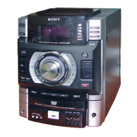
HCD-GN1300D
75
63, 64 HA18, HA19 O Host address output bit 18, 19
65 DVDD3 – Power supply pin (+3.3 V) for internal digital circuitry
66 XWR O Write enable output (active Low)
67 to 74 HA16 to HA9 O Host address output bit 16 to 9
75 HA20 O Host address output bit 20
76 XROMCS O Chip select output (active Low)
77 HA1 O Host address output bit 1
78 XRD O Read enable output (active Low)
79, 80 HD0, HD1 O Host data output bit 0, 1
81 DVSS – Ground pin for internal digital circuitry
82 to 86 HD2 to HD6 O Host data output bit 2 to 6
87 HA21 O Host address output bit 21
88 RESERVED O Not used. (Open)
89 HD7 O Host data output bit 7
90 DVSS – Ground pin for internal digital circuitry
91 HA17 O Host address output bit 17
92 HA0 O Host address output bit 0
93 DVDD18 – Power supply pin (+1.8 V) for internal digital circuitry
94 FWD O Forward signal output for loading motor driver (Not used in this set)
95 REV O Reserve signal output for loading motor driver (Not used in this set)
96 DVDD3 – Power supply pin (+3.3 V) for internal digital circuitry
97 IFSDO O External CPU serial data output (H/W method)
98 IFCK O External CPU serial clock output (H/W method)
99 xIFCS O External CPU serial chip select output (active Low, H/W method)
100 IFSDI I External CPU serial data input (H/W method)
101 SCL O I2C clock output for EEPROM
102 SDA O I2C data output for EEPROM
103 CKSW I Chucking switch detection input (Not used in this set)
104 OCSW I Open/close switch detection input (Not used in this set)
105 RXD I Hardwired RS232C RXD input
106 TXD O Hardwired RS232C TXD output
107 ICE I ICE mode enable input (Not used in this set)
108 xSYSRST I MT1389 reset input (active Low)
109 RESERVED I Not used. (Open)
110 xIFBSY I External CPU ready/busy interrupt signal input (L: ready, H: busy)
111 DQM0 O Mask for DRAM output byte 0
112 EEWP O EEPROM write protect control output (L: write allowed)
113 to 117 RD7 to RD3 O DRAM data output bit 7 to 3
118 DVDD3 – Power supply pin (+3.3 V) for internal digital circuitry
119 to 121 RD2 to RD0 O DRAM data output bit 2 to 0
122 to 129 RD15 to RD8 O DRAM data output bit 15 to 8
130 TSD_M I Thermal shutdown monitor input
131 DVDD3 – Power supply pin (+3.3 V) for internal digital circuitry
132 DQM1 O Mask for DRAM output byte 1
133 _RWE O DRAM write enable output
134 _CAS O DRAM column address strobe output
135 _RAS O DRAM row address strobe output
136 _RCS O DRAM chip select output
137, 138 BA0, BA1 O DRAM bank address output 0, 1
139 RA10 O DRAM address output bit 10
140, 141 RA0, RA1 O DRAM address output bit 0, 1
142 DVDD18 – Power supply pin (+1.8 V) for internal digital circuitry
143, 144 RA2, RA3 O DRAM address output bit 2, 3
145 DVDD3 – Power supply pin (+3.3 V) for internal digital circuitry
146 DRCLK O DRAM clock output
147 CKE O DRAM clock enable output
148 DVSS – Ground pin for internal digital circuitry