Note:
The components identi-
fied by mark 0 or dotted
line with mark 0 are criti-
cal for safety.
Replace only with part
number specified.
Note:
Les composants identifiés par
une marque 0 sont critiques
pour la sécurité.
Ne les remplacer que par une
piéce portant le numéro
spécifié.
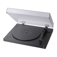
PMC-DR45
– 33 – – 34 –
6-7. PRINTED WIRING BOARD — TUNER SECTION —
THIS NOTE IS COMMON FOR PRINTED WIRING
BOARDS AND SCHEMATIC DIAGRAMS.
(In addition to this, the necessary note is
printed in each block.)
for Schematic Diagram:
• All capacitors are in µF unless otherwise noted. pF: µµF
50 WV or less are not indicated except for electrolytics
and tantalums.
• All resistors are in Ω and
1
/4
W or less unless otherwise
specified.
• % : indicates tolerance.
•
f
: internal component.
• C : panel designation.
Caution:
Pattern face side: Parts on the pattern face side seen from
(Conductor Side) the pattern face are indicated.
Parts face side: Parts on the parts face side seen from
(Component Side) the parts face are indicated.
• U : B+ Line.
• V : B– Line.
• H : adjustment for repair.
• Voltages are taken with a VOM (Input impedance 10 MΩ).
Voltage variations may be noted due to normal produc-
tion tolerances.
• Waveforms are taken with a oscilloscope.
Voltage variations may be noted due to normal produc-
tion tolerances.
• Circled numbers refer to waveforms.
• Signal path.
F : FM
f : AM
L : LINE
E : PB
a : REC
J : CD
c : digital out
for Printed Wiring Boards:
• X : parts extracted from the component side.
• Y : parts extracted from the conductor side.
•
a
: Through hole.
• b : Pattern from the side which enables seeing.
(The other layer’s patterns are not indicated.)
D1 B-8
D2 B-8
D3 C-5
D4 B-6
D5 D-6
IC1 E-7
IC2 D-3
• Semiconductor
Location
Ref. No. Location
1
A
B
C
D
E
F
234567891011
-2
EXT ANT
-1
AM
TP(VT)
TM1
1
MAIN BOARD
CNP305
1-677-166-
(11)
11
(Page 45)