5353
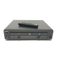
RCD-W10
• Waveform
For schematic diagrams.
Note:
• All capacitors are in µF unless otherwise noted. p : pF. 50 WV or
less are not indicated except for electrolytics and tantalums.
• All resistors are in Ω and
1
/
4
W or less unless otherwise specified.
•
f
: internal component.
• C : panel designation.
• A : B+ Line.
• B : B– Line.
• H : adjustment for repair.
•Voltages and waveforms are dc with respect to ground under no-
signal (detuned) conditions.
No mark : STOP
•Voltages are taken with a VOM (Input impedance 10 MΩ).
Voltage variations may be noted due to normal production toler-
ances.
•Waveforms are taken with a oscilloscope.
Voltage variations may be noted due to normal production toler-
ances.
• Circled numbers refer to waveforms.
• Signal path.
J : CD PLAY
E : CD-R PLAY (ANALOG OUT)
a : CD-R REC (ANALOG IN)
k : CD-R REC (CD)
For printed wiring boards.
Note:
• X : parts extracted from the component side.
• Y : parts extracted from the conductor side.
•
a
: Through hole.
• : Pattern from the side which enables seeing.
(The other layers' patterns are not indicated.)
• Indication of transistor
THIS NOTE IS COMMON FOR PRINTED WIRING
BOARDS AND SCHEMATIC DIAGRAMS.
(In addition to this necessary note is printed in
each block.)
Note:
The components identified by
mark 0 or dotted line with mark
0 are critical for safety.
Replace only with part number
specified.
Note:
Les composants identifiés par
une marque 0 sont critiques
pour la sécurité.
Ne les remplacer que par une
pièce portant le numéro spécifié.
CEB
These are omitted.
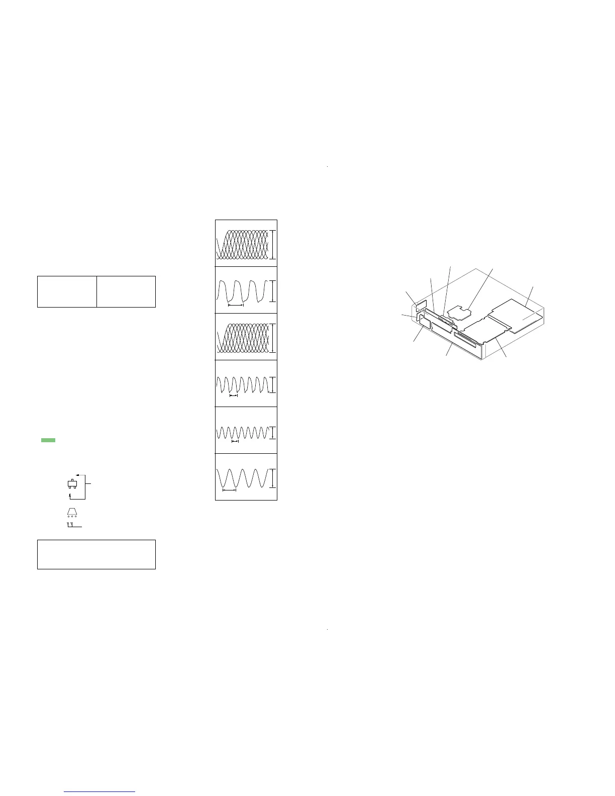
1 IC103 qg (RFAC)
200mV/DIV, 400ns/DIV
1.2Vp-p
1V/DIV, 10ns/DIV
2 IC101 us (XTAO)
4.4Vp-p29.5ns
3 IC101 i; (EQRF)
200mV/DIV, 400ns/DIV
1.4Vp-p
4 IC201 <zn, (XTAL)
2V/DIV, 20ns/DIV
6.4Vp-p29.5ns
5 IC501 yj (XTAL)
1V/DIV, 40ns/DIV
2.4Vp-p50ns
6 IC1 ek (X2)
1V/DIV, 20ns/DIV
3.9Vp-p50ns
• Circuit Board Location
SECTION 6
DIAGRAMS
C
B
These are omitted.
E
Q
Caution:
Pattern face side: Parts on the pattern face side seen from
(Conductor B) the pattern face are indicated.
Parts face side: Parts on the parts face side seen from
(Component A) the parts face are indicated.
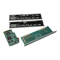
LOADING board
POWER-SW board
CD-SW board
CD-EJECT board
DISPLAY board
MAIN boar
 Loading...