5. Schematic Diagrams
5-25-1
5-1 S.M.P.S (VCR Main PCB) - - - - - - - - - - - - - - - - - - - - - - - - - - - - - - - - - 5-3
5-2 Power (VCR Main PCB) - - - - - - - - - - - - - - - - - - - - - - - - - - - - - - - - - - 5-5
5-3 Logic (VCR Main PCB) - - - - - - - - - - - - - - - - - - - - - - - - - - - - - - - - - - - 5-7
5-4 A/V (VCR Main PCB) - - - - - - - - - - - - - - - - - - - - - - - - - - - - - - - - - - - - 5-9
5-5 Hi-Fi (VCR Main PCB) - - - - - - - - - - - - - - - - - - - - - - - - - - - - - - - - - - - 5-11
5-6 Function Timer (Function Timer PCB) - - - - - - - - - - - - - - - - - - - - - - - - - 5-13
5-7 Encoder (DVD Jack Main PCB) - - - - - - - - - - - - - - - - - - - - - - - - - - - - - 5-15
5-8 Decoder (DVD Jack Main PCB) - - - - - - - - - - - - - - - - - - - - - - - - - - - - - 5-17
5-9 Video Decoder and Connector (DVD Jack Main PCB) - - - - - - - - - - - - - - 5-19
5-10 DV Interface and 1394 Connector (DVD Jack Main PCB) - - - - - - - - - - - - 5-21
5-11 Component/Super Out (Front Jack PCB) - - - - - - - - - - - - - - - - - - - - - - - 5-23
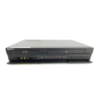
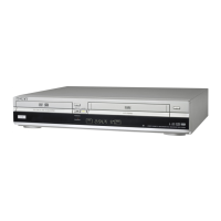
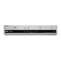
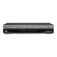
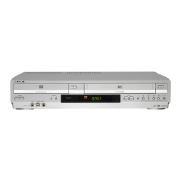
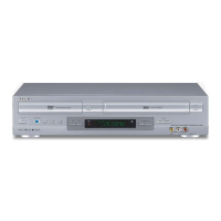
RDR-VX521/VX530
Note
For schematic Diagram
- Resistors are in ohms, 1/8W unless otherwise noted.
Special note :
Most semiconductor devices are electrostatically sensitive and therefore require the special handling techniques described under the
“electrostatically sensitive (ES) devices” section of this service manual.
Important safety notices :
Components identified with the mark 0 have the special characteristics for safety. When replacing any of these components.
Use only the same type.