141
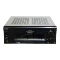
STR-DA5300ES
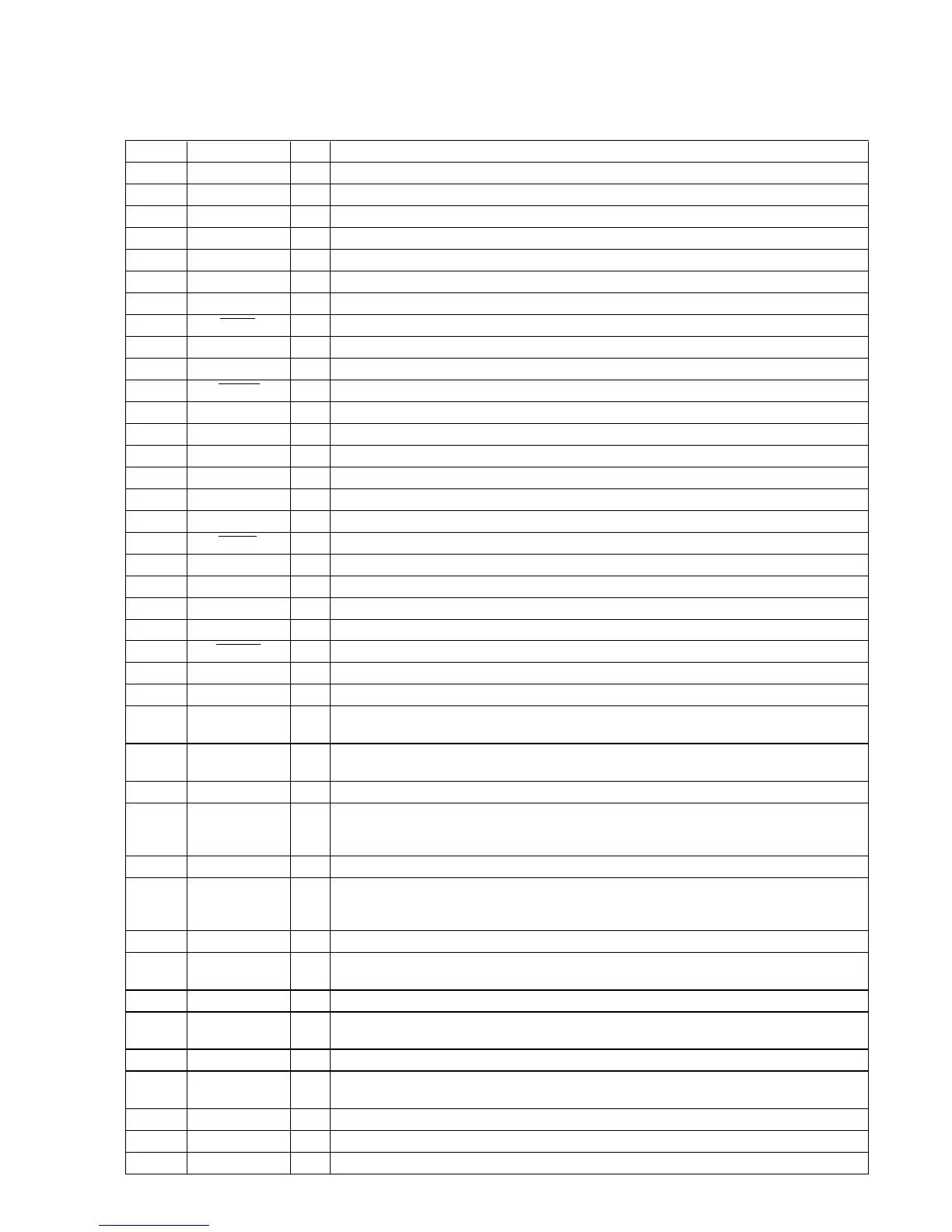
• IC Pin Function Description
DSP BOARD IC5002 ADSST-AVR-1132 (DSP1)
Pin No. Pin Name I/O Description
A1
CLKCFG0 I Clock frequency setting terminal
XTAL O System clock output terminal (12.288 MHz)
MOSI I Serial data input from the DSP controller
MISO O Serial data output to the DSP controller
SPIDS I Serial data latch pulse signal input from the DSP controller
VDDINT - Power supply terminal (+1.2V)
CLKCFG1 I Clock frequency setting terminal
VDDEXT - Power supply terminal (+3.3V)
CLKIN I System clock input terminal (12.288 MHz)
AVDD - Power supply terminal (+1.2V)
VDDEXT - Power supply terminal (+3.3V)
SPICLK I Serial data transfer clock signal input from the DSP controller
RESET I Reset signal input from the DSP controller "L": reset
VDDINT - Power supply terminal (+1.2V)
BOOTCFG1,
BOOTCFG0
I Boot mode setting signal input from the DSP controller
C3, C12,
C13
GND - Ground terminal
VDDINT - Power supply terminal (+1.2V)
D2, D4 to
D6, D9 to
D11, D13
GND - Ground terminal
VDDINT - Power supply terminal (+1.2V)
E2, E4 to
E6, E9 to
E11, E13
GND - Ground terminal
P_ERROR O PLL lock error signal and data error flag output to the DSP2 and DSP controller
FLAG1 I
Audio muting control signal input from the digital audio interface receiver, video system controller
or HDMI receiver
FLAG0 O Interrupt request signal output to the DSP controller
F4 to F6,
F9 to F11
GND - Ground terminal
PCM audio data input from the digital audio interface receiver or video system controller
Master clock signal input from the digital audio interface receiver, digital audio processor, HDMI
receiver or XM receiver
Two-way data bus with S-RAM and flash memory and address signal output to the address latch
VDDINT - Power supply terminal (+1.2V)
VDDEXT - Power supply terminal (+3.3V)