142
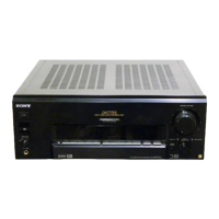
STR-DA5300ES
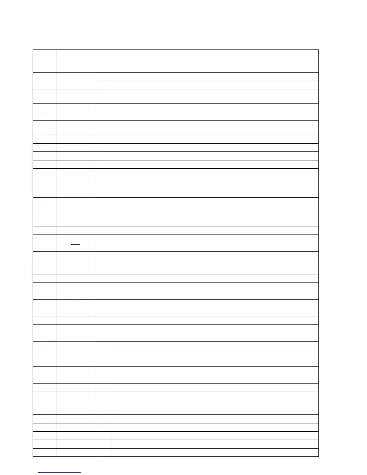
Pin No. Pin Name I/O Description
G14 DPBCK I
Bit clock signal input for PCM audio input from the digital audio interface receiver, digital audio
processor, HDMI receiver or XM receiver
H1 AD6 I/O
Two-way data bus with S-RAM and flash memory and address signal output to the address latch
H2
VDDEXT - Power supply terminal (+3.3V)
H13 DPLRCK I
L/R sampling clock signal input for PCM audio input from the digital audio interface receiver,
digital audio processor, HDMI receiver or XM receiver
H14 DPDVBCK O
Bit clock signal output for PCM audio output to the DSP2
J1, J2 AD5, AD4 I/O
Two-way data bus with S-RAM and flash memory and address signal output to the address latch
J4 to J6,
J9 to J11
GND - Ground terminal
J13
VDDINT - Power supply terminal (+1.2V)
J14 DPDVLRCK O
L/R sampling clock signal output for PCM audio output to the DSP2
K1 AD3 I/O
Two-way data bus with S-RAM and flash memory and address signal output to the address latch
K2
VDDINT - Power supply terminal (+1.2V)
K4 to K6,
K9 to K11,
K13
GND - Ground terminal
K14 DPSIE I
PCM audio signal (surround back L/R) input from the HDMI receiver
L1, L2 AD2, AD1 I/O
Two-way data bus with S-RAM and flash memory and address signal output to the address latch
L4 to L6,
L9 to L11,
L13
GND - Ground terminal
L14 DPSID I
PCM audio signal (center, sub woofer) input from the HDMI receiver
M1 AD0 I/O
Two-way data bus with S-RAM and flash memory and address signal output to the address latch
M2 WR O
Data write enable signal output to the S-RAM and flash memory
M3, M12
GND - Ground terminal
M13 DPSIB I
PCM audio signal (front L/R) input from the A/D converter, digital audio processor, HDMI
receiver or XM receiver
M14 DPSIC I
PCM audio signal (surround L/R) input from the HDMI receiver or digital audio processor
N1 AD15 O
Address signal output to the S-RAM and flash memory
N2 ALE O
Address latch enable signal output terminal
N3
RD
O
Data read enable signal output to the S-RAM and flash memory
N4
VDDINT - Power supply terminal (+1.2V)
N5
VDDEXT - Power supply terminal (+3.3V)
N6 AD8 O
Address signal output to the S-RAM, flash memory and address latch
N7
VDDINT - Power supply terminal (+1.2V)
N8
DAI_P2 - Not used
N9
VDDEXT - Power supply terminal (+3.3V)
N10
DAI_P4 - Not used
N11, N12
VDDINT - Power supply terminal (+1.2V)
N13
GND - Ground terminal
N14
DPSOE O PCM audio signal output to the DSP2
P1 to P6 AD14 to AD9 O
Address signal output to the S-RAM, flash memory and address latch
P7, P8, P9
DAI_P1, DAI_P3,
DAI_P5
- Not used
P10 DPSOA O
PCM audio signal (front L/R) output to the DSP2
P11 DPSOB O
PCM audio signal (surround L/R) output to the DSP2
P12 DPSOC O
PCM audio signal (center, sub woofer) output to the DSP2
P13 DPSOD O
PCM audio signal (surround back L/R) output to the DSP2
P14 DPSIA I
PCM audio signal (digital input) input from the digital audio interface receiver