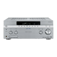
STR-DA5500ES
160
NETWORK BOARD IC8013 PNX1502E/G, 557 (CONNECTED MEDIA PROCESSOR)
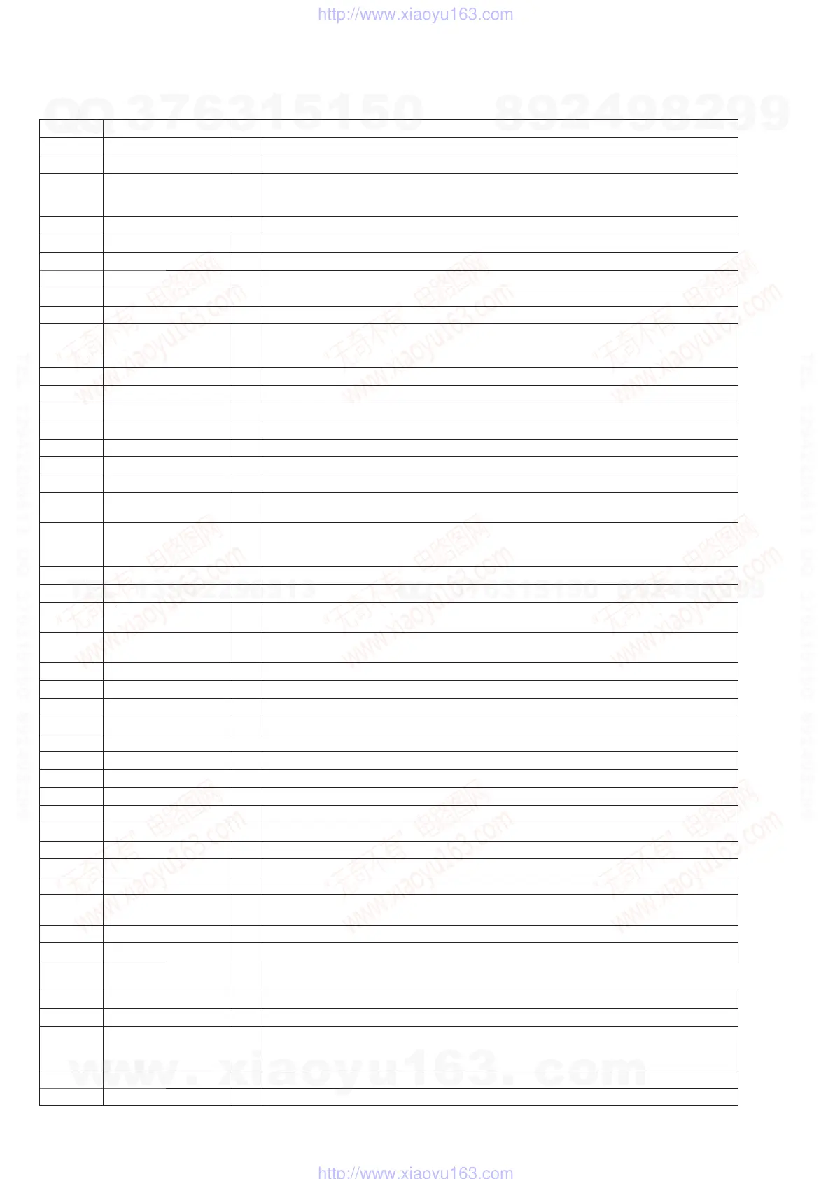
Pin No. Pin Name I/O Description
A1 JTAG_TDI I Data input terminal (for JTAG) Not used
A2 VCCP - Power supply terminal (+3.3V)
A3, A4
CLOCK02/BOOT_
MODE02, CLOCK03/
BOOT_MODE03
- Not used
A5 VSSA - Ground terminal
A6 SPDI - Not used
A7 CLOCK04 O Data selection signal output terminal
A8 CLOCK05 O Relay drive signal (for main power) output terminal “H”: relay on
A9 VSS - Ground terminal
A10 VDDA - Power supply terminal (+1.3V)
A11 POR_IN_N I
System reset signal input from the reset signal generator “L”: reset
For several hundreds msec. after the power supply rises, “L” is input, then it changes to “H”
Reset signal input from the system controller “L”: reset
A12 VDD - Power supply terminal (+1.3V)
A13 VSS - Ground terminal
A14 VSSA - Ground terminal
A15 VDD - Power supply terminal (+1.3V)
A16 VCCA - Power supply terminal (+3.3V)
A17 VDD - Power supply terminal (+1.3V)
A18 FGPO_BUF_SYNC - Not used
A19 to A21
VDD_D33, VDD_D00,
VDD_D01
O Digital video signal output terminal Not used
A22 to A26
VDO_D05, VDO_D09,
VDO_D14, VDO_D16,
VDO_D17
O Digital video signal output to the D/A converter (for network (video) section)
B1 JTAG_TCK I Clock signal input terminal (for JTAG) Not used
B2 VDD_D34 O Digital video signal output terminal Not used
B3
CLOCK01/
BOOT_MODE01
O Emphasis control signal output to the D/A converter (for network (audio) section)
B4
CLOCK00/
BOOT_MODE00
O Muting control signal output terminal
B5 VCCA - Power supply terminal (+3.3V)
B6 VCCP - Power supply terminal (+3.3V)
B7 VSS - Ground terminal
B8 VSSA - Ground terminal
B9 CLOCK06 O LED drive signal output terminal for MULTI CHANNEL DECODING indicator “H”: LED on
B10 to B12 VSS - Ground terminal
B13 VSSA - Ground terminal
B14 VDD - Power supply terminal (+1.3V)
B15, B16 VSSA - Ground terminal
B17 VSS - Ground terminal
B18 VDD_D32 O Digital video signal output terminal Not used
B19 VDO_CLK2 O Clock signal output terminal Not used
B20 VDO_D02 O Digital video signal output terminal Not used
B21 to B24
VDO_D06, VDO_D07,
VDO_D11, VDO_D15
O Digital video signal output to the D/A converter (for network (video) section)
B25 VSS - Ground terminal
B26 VDO_D21 O Digital video signal output to the D/A converter (for network (video) section)
C1 to C3
MM_DATA01, MM_
DATA00, MM_DATA15
I/O Two-way data bus with the SD-RAM
C4, C5 VSS - Ground terminal
C6 VDD - Power supply terminal (+1.3V)
C7 RESET_IN_N I
System reset signal input from the reset signal generator “L”: reset
For several hundreds msec. after the power supply rises, “L” is input, then it changes to “H”
Reset signal input from the system controller “L”: reset
C8 IIC_SDA I/O Two-way I2C data bus with the EEPROM and D/A converter (for network (video) section)
C9, C10 VDD - Power supply terminal (+1.3V)
w
w
w
.
x
i
a
o
y
u
1
6
3
.
c
o
m
Q
Q
3
7
6
3
1
5
1
5
0
9
9
2
8
9
4
2
9
8
T
E
L
1
3
9
4
2
2
9
6
5
1
3
9
9
2
8
9
4
2
9
8
0
5
1
5
1
3
6
7
3
Q
Q
TEL 13942296513 QQ 376315150 892498299
TEL 13942296513 QQ 376315150 892498299
http://www.xiaoyu163.com
http://www.xiaoyu163.com