STR-DA5500ES
161
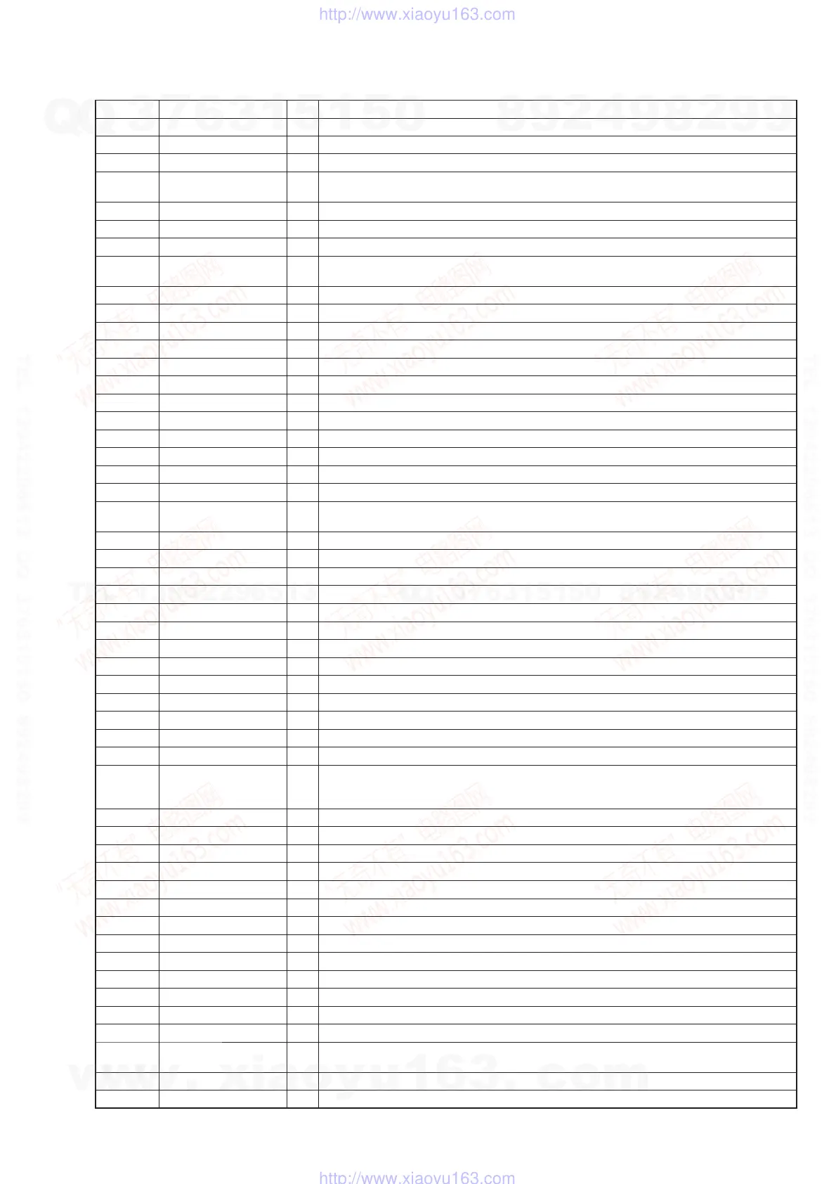
Pin No. Pin Name I/O Description
C11 VSSA_1.2 - Ground terminal
C12 VCCP - Power supply terminal (+3.3V)
C13 VCCA - Power supply terminal (+3.3V)
C14 to
C16
VSS - Ground terminal
C17 FGPO_REC_SYNC O Not used
C18 VCCP - Power supply terminal (+3.3V)
C19 VDO_D03 O Digital video signal output terminal Not used
C20 to
C23
VDO_D08, VDO_D10,
VDO_D12, VDO_D18
O Digital video signal output to the D/A converter (for network (video) section)
C24 VCCP - Power supply terminal (+3.3V)
C25 VDO_D22 O Digital video signal output to the D/A converter (for network (video) section)
C26 VDO_D31 O Blanking signal output to the D/A converter (for network (video) section)
D1 MM_DATA03 I/O Two-way data bus with the SD-RAM
D2 VCCM - Power supply terminal (+2.6V)
D3 MM_DATA14 I/O Two-way data bus with the SD-RAM
D4 VCCM - Power supply terminal (+2.6V)
D5 JTAG_TMS I Mode selection signal input terminal (for JTAG) Not used
D6 JTAG_TDO O Data output terminal (for JTAG) Not used
D7 VCCA - Power supply terminal (+3.3V)
D8 IIC_SCL O I2C clock signal output to the EEPROM and D/A converter (for network (video) section)
D9 XTAL_OUT O System clock output terminal Not used
D10 SYS_RST_OUT_N O
Reset signal output to the ethernet interface, D/A converter (for network (video) section),
parallel bus/I2C bus converter and pararell/serial converter “L”: reset
D11 XTAL_IN I System clock input terminal (27 MHz)
D12, D13 VDD - Power supply terminal (+1.3V)
D14, D15 VCCA - Power supply terminal (+3.3V)
D16 VDO_D04 O Digital video signal output terminal Not used
D17 VDO_D13 O Digital video signal output to the D/A converter (for network (video) section)
D18 VDO_CLK1 O Serial data transfer clock signal output to the D/A converter (for network (video) section)
D19 VDO_D23 O Digital video signal output to the D/A converter (for network (video) section)
D20 VDO_D29 O Vertical sync signal output to the D/A converter (for network section)
D21, D22 VDO_D19, VDO_D20 O Digital video signal output to the D/A converter (for network (video) section)
D23 PCI_INTA_N I Interrupt signal input terminal Not used
D24 PCI_GNT_N I Grant signal input terminal Not used
D25 PCI_GNT_A_N I Interrupt signal input from the parallel bus/I2C bus converter
D26 PCI_GNT_B_N I Grant signal input terminal Not used
E1 to E4
MM_DATA04, MM_
DATA02, MM_DATA12,
MM_DATA13
I/O Two-way data bus with the SD-RAM
E5, E6 VSS - Ground terminal
E7, E8 VCCP - Power supply terminal (+3.3V)
E9, E10 VDD - Power supply terminal (+1.3V)
E11, E12 VSS - Ground terminal
E13, E14 VCCP - Power supply terminal (+3.3V)
E15, E16 VDD - Power supply terminal (+1.3V)
E17, E18 VSS - Ground terminal
E19, E20 VCCP - Power supply terminal (+3.3V)
E21, E22 VSS - Ground terminal
E23 PCI_CLK I System clock input terminal (27 MHz)
E24 VDO_AUX O Not used
E25 PCI_SYS_CLK O Not used
E26 VDO_D30 O Horizontal sync signal output to the D/A converter (for network (video) section)
F1 to F3
MM_DATA06, MM_
DATA05, MM_DATA11
I/O Two-way data bus with the SD-RAM
F4, F5 VSS - Ground terminal
F22 VSS - Ground terminal
w
w
w
.
x
i
a
o
y
u
1
6
3
.
c
o
m
Q
Q
3
7
6
3
1
5
1
5
0
9
9
2
8
9
4
2
9
8
T
E
L
1
3
9
4
2
2
9
6
5
1
3
9
9
2
8
9
4
2
9
8
0
5
1
5
1
3
6
7
3
Q
Q
TEL 13942296513 QQ 376315150 892498299
TEL 13942296513 QQ 376315150 892498299
http://www.xiaoyu163.com
http://www.xiaoyu163.com