General-purpose timers (TIM15/TIM16/TIM17) RM0440
1362/2126 RM0440 Rev 4
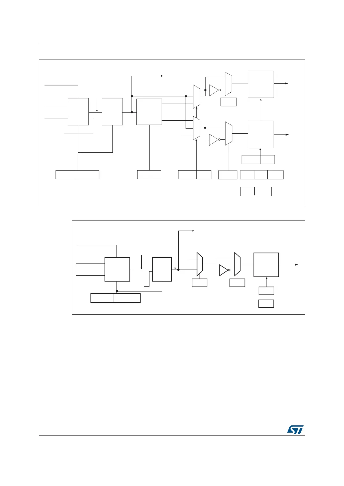
Figure 455. Output stage of capture/compare channel (channel 1)
Figure 456. Output stage of capture/compare channel (channel 2 for TIM15)
The capture/compare block is made of one preload register and one shadow register. Write
and read always access the preload register.
In capture mode, captures are actually done in the shadow register, which is copied into the
preload register.
In compare mode, the content of the preload register is copied into the shadow register
which is compared to the counter.
30.4.8 Input capture mode
In Input capture mode, the Capture/Compare Registers (TIMx_CCRx) are used to latch the
value of the counter after a transition detected by the corresponding tim_icx signal. When a
capture occurs, the corresponding CCXIF flag (TIMx_SR register) is set and an interrupt or
a DMA request can be sent if they are enabled. If a capture occurs while the CCxIF flag was
MSv62366V2
Output
mode
controller
CNT>CCR1
CNT=CCR1
TIMx_CCMR1
OC1M[3:0]
tim_oc1ref
OC1CE
Dead-time
generator
tim_oc1_dt
tim_oc1n_dt
DTG[7:0]
TIMx_BDTR
‘0’
‘0’
CC1E
TIMx_CCER
CC1NE
0
1
CC1P
TIMx_CCER
0
1
CC1NP
TIMx_CCER
tim_oc1
Output
enable
circuit
tim_oc1n
CC1E
TIMx_CCER
CC1NE
OSSI
TIMx_BDTR
MOE OSSR
0x
10
11
11
01
x0
Output
selector
tim_oc2ref
tim_oc1refc
To the master mode
controller
Output
enable
circuit
OIS1N
TIMx_CR2
OIS1
tim_ocref_clr_int
MSv62367V2
Output
mode
controller
CNT > CCR2
CNT = CCR2
TIMx_CCMR1
OC2M[3:0]
0
1
CC2P
TIMx_CCER
Output
enable
circuit
tim_oc2
CC2E
TIMx_CCER
To the master
mode controller
tim_oc2ref
Output
selector
tim_oc1ref
OC2CE
0
1
CC2E
TIMx_CCER
tim_oc2refc
‘0’
OIS2
TIMx_CR2
tim_ocref_clr_int

 Loading...


