RM0440 Rev 4 1949/2126
RM0440 FD controller area network (FDCAN)
2008
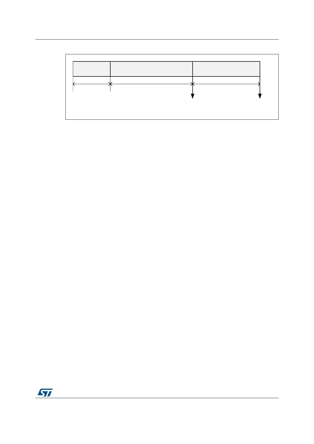
Figure 664. Bit timing
The baud rate is the inverse of bit time (baud rate = 1 / bit time), which, in turn, is the sum of
three components. Figure 664 indicates that bit time = t
SyncSeg
+ t
BS1
+ t
BS2
, where:
• for the nominal bit time
– tq = (FDCAN_NBTP.NBRP[8:0] + 1) * t
fdcan_tq_clk
–t
SyncSeg
= 1 tq
–t
BS1
= tq * (FDCAN_NBTP.NTSEG1[7:0] + 1)
–t
BS2
= tq * (FDCAN_NBTP.NTSEG2[6:0] + 1)
• for the data bit time
– tq = (FDCAN_DBTP.DBRP[4:0] + 1) * t
fdcan_tq_clk
–t
SyncSeg
= 1 tq
–t
BS1
= tq * (FDCAN_DBTP.DTSEG1[4:0] + 1)
–t
BS2
= tq * (FDCAN_DBTP.DTSEG2[3:0] + 1)
The (Re)Synchronization Jump Width (SJW) defines an upper bound for the amount of
lengthening or shortening of the bit segments. It is programmable between one and four
time quanta.
A valid edge is defined as the first transition in a bit time from dominant to recessive bus
level, provided the controller itself does not send a recessive bit.
If a valid edge is detected in BS1 instead of SYNC_SEG, BS1 is extended by up to SJW so
that the sample point is delayed.
Conversely, if a valid edge is detected in BS2 instead of SYNC_SEG, BS2 is shortened by
up to SJW so that the transmit point is moved earlier.
As a safeguard against programming errors, the configuration of the Bit Timing register is
only possible while the device is in Standby mode. Registers FDCAN_DBTP and
FDCAN_NBTP (dedicated, respectively, to data and nominal bit timing) are only accessible
when CCCR.CCE and CCCR.INIT are set.
Note: For a detailed description of the CAN bit timing and resynchronization mechanism, refer to
the ISO 11898-1 standard.
44.3.2 Operating modes
Configuration
Access to IP version, hardware and input clock divider configuration. When the clock divider
is set to 0, the primary input clock is used as it is.
MS47283V1
SyncSeg Bit segment 1 (BS1) Bit segment 2 (BS2)
t
SyncSeg
t
BS2
t
BS1
Sample
point
Transmit
point

 Loading...


