RM0440 Rev 4 515/2126
RM0440 Flexible static memory controller (FSMC)
571
At startup the FMC pins must be configured by the user application. The FMC I/O pins which
are not used by the application can be used for other purposes.
The FMC registers that define the external device type and associated characteristics are
usually set at boot time and do not change until the next reset or power-up. However, the
settings can be changed at any time.
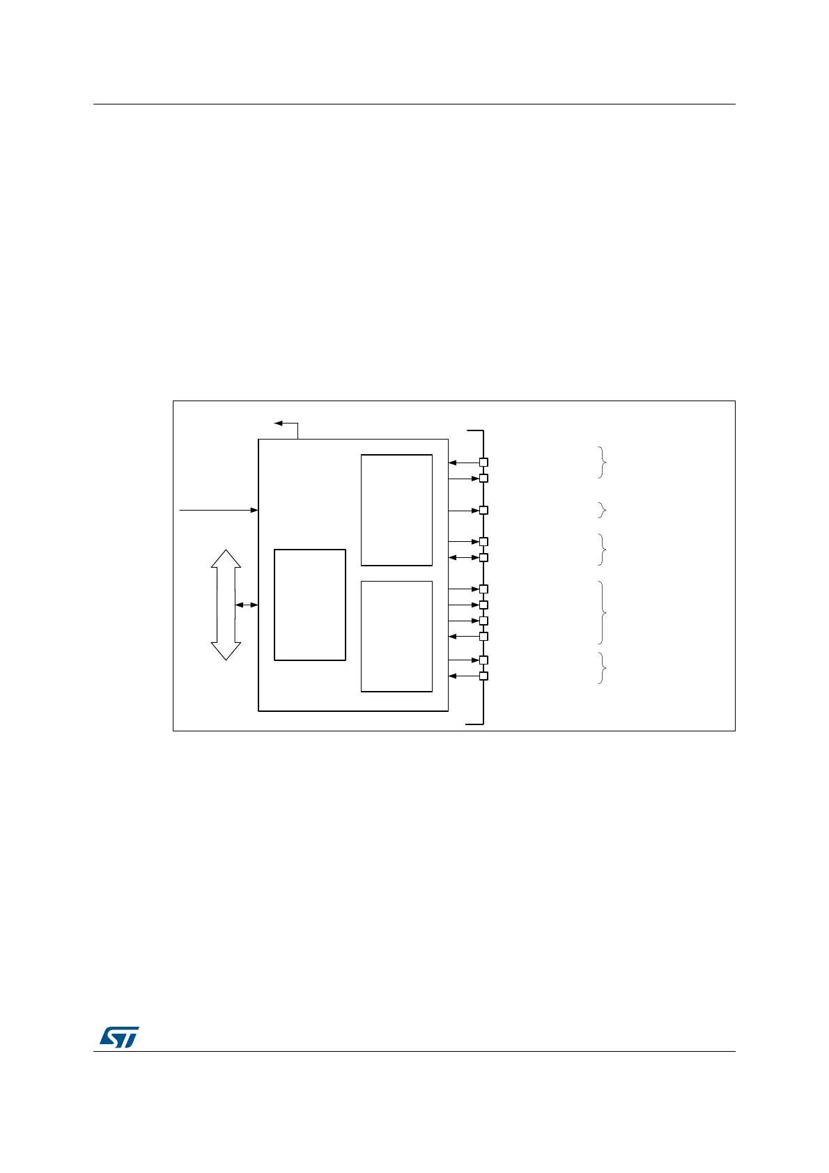
19.3 FMC block diagram
The FMC consists of the following main blocks:
• The AHB interface (including the FMC configuration registers)
• The NOR Flash/PSRAM/SRAM controller
The block diagram is shown in the figure below.
Figure 52. FMC block diagram
MS34473V3
NOR/PSRAM
signals
FMC_NE[4:1]
FMC_NL (or NADV)
FMC_D[15:0]
FMC_NOE
FMC_NWE
FMC_NBL[1:0]
FMC_NCE
FMC_INT
FMC_CLK
FMC_A[25:0]
FMC interrupts to NVIC
From clock
controller
NOR/PSRAM
memory
controller
Configuration
registers
NAND
memory
controller
HCLK
FMC_NWAIT
NAND signals
NOR / PSRAM / SRAM
shared signals
Shared signals
NOR / PSRAM / SRAM
shared signals

 Loading...


