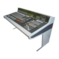
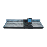
3.3.2 Input unit mono 1.928.220
Distortion:
• Feed test signal with nominal level (1 kHz, typ. +6 or +10 dBu)
to the LINE input.
• Set the LINE GAIN and PAN potentiometers to their center
positions (CAL.), switch filters off, and set the fader to its 0 dB
position.
• Remove the Input unit from the console and reconnect it via
the bus adapter (optionally available; order no. 1.228.332.00).
• Route the signal to Master A (ΣA).
• Connect the distortion analyzer to the PF INSERT SEND con-
nector of Master unit A.
• Adjust VR14 to minimum distortion (typical value: <80 dB @
1 kHz).
Level:
• Connect the AF voltmeter to the PF INSERT SEND connector
of Master unit A.
• Adjust the level with trimmer potentiometer VR16 to 3 dB be-
low nominal level.
Meter PPM (JP7 set to 1-2, see section 3.1.1):
• Feed test signal with nominal level (1 kHz, typ. +6 or +10 dBu)
to the LINE input.
• Adjust trimmer potentiometer VR12 to 0 dB indication.
Meter VU (JP7 set to 2-3, see section 3.1.1):
• Feed test signal with nominal level –6 dB (1 kHz, typ. 0 or
+4 dBu) to the LINE input.
• Adjust trimmer potentiometer VR12 to 0 dB indication.
Note: Usually, a 6 dB lead is used to compensate for the low-
er rise time of the VU meter (example: If the nominal level is
+10 dBu, 0 VU is indicated with an input level of +4 dBu).
Direct output:
• Connect the AF voltmeter to the DIRECT OUTPUT.
• Route the signal to Master A (ΣA).
• Press the N-1 switch (“clean feed”).
• Adjust the output to minimum level with trimmer potentiome-
ter VR15.
• Press the Master A routing switch (ΣA).
• Adjust the output signal to minimum level with trimmer poten-
tiometer VR13.
Generator:
• Select the generator (“~”) in the input selector section.
• Switch the generator ON on the Studio Monitor module, set
the frequency to 1 kHz.
• Connect the AF voltmeter to the PF INSERT SEND connector
of Master unit A.
• Set the PAN potentiometer to its center position and the fader
to its 0 dB position.
• Adjust RA1 on the INPUT SIDE SWITCH BOARD to 3 dB be-
low nominal level.
LK5
LK6
J2
J1
J9
J13
J14
VR13
VR15
N-1
SUM
NULL1
N-1
NULL2
J4
J3
J5
VR12
METER
J7
VR14
VR16
J12
LK4
LK3
LK2
LK1
J10 J8
J11
J6
LK7
LK8
Main Board
1.928.220
(component side)