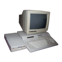
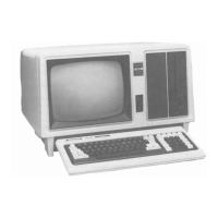
Tandy 1000
Technical Reference Manual
inter
8237A/8237A-4/8237
A-5
Table
1.
Pin
Description
(Continued)
,------.----,------------,
,------r---r---------~
Symbol
Name and
Function
Symbol Type Name and Function
A4-A7
0 Addre
..
:
The
four most significant
address lines
are
three-state out-
puts
and
provide 4 bits of
address.
These
lines
are
enabled only during
the
DMA
service.
HRQ
0 Hold Reque.t: This
Is
the
Hold
Re-
quest to the
CPU
and
Is
used
to
re-
quest control of
the
system bus. If
the corresponding mask bit
Is
clear, the presence of
any
valid
DREQ
causes
8237
A to issue the
HRQ.
After
HRQ
goes active at
least
one
clock cycle (lCY) must
occur before
HlDA
goes active.
DACKo-DACK3
0
OMA
Acknowledge:
DMA Ac-
knowledge
is
used
to notify
the
in-
dividual peripherals
when
one
has
been granted a
DMA
cycle. The
sense
of these lines
is
program-
mable.
Reset
initializes them to
ac-
tive low.
FUNCTIONAL DESCRIPTION
AEN
ADSTB
MEMW
o Addre
••
Enable: Address Enable
enables the B-bit latch containing
the upper 8 address bits onto
the
system
address
bus.
AEN
can
also
be
used
to disable other
system
bus
drivers during
DMA
transfers.
AEN
is
active
HIGH.
o Addre
••
Strobe:
The
active high,
Address Strobe
is
used
to strobe
the
upper address byte into
an
external
latch.
o Memory Read:
The
Memory
Read
signal
is
an
active low three-state
output used to
access
data from the
selected memory location during a
DMA
Read
or amemory-ta-memory
transfer.
o Memory Write:
The
Memory Write
is
an
active iow three-state output
used
to write
data
to the selected
memory location during a
DMA
Write
or
a memory-to-memory
transfer.
The
Timing
Control
block
derives
internal
timing
from
the
clock
input.
In 8237A
systems
this
input
will
usually
The 8237A
block
diagram
includes
the
major
logic
blocks
and
all
of
the
internal
registers.
The
data
inter-
connection
paths
are
also
shown.
Not
shown
are
the
various
control
signals
between
the
blocks.
The 8237A
contains
344
bits
of
internal
memory
in
the
form
of
registers.
Figure
3
lists
these
registers
by name and
shows
the
size
of
each. A
detailed
description
of
the
registers
and
their
functions
can be
found
under
Register
Description.
Figure
3.
8237A
Internal
Registers
The 8237A
contains
three
basic
blocks
of
control
logic.
The
Timing
Control
block
generates
internal
timing
and
external
control
signals
for
the
8237A. The Program
Command
Control
block
decodes
the
various
com-
mands
given
to
the
8237A
by
the
microprocessor
prior
to
servicing
a
DMA
Request. It
also
decodes
the
Mode
Control
word
used
to
select
the
type
of
DMA
during
the
servicing.
The
Priority
Encoder
block
resolves
priority
contention
between
DMA
channels
requesting
service
simultaneously.
Base
Address
Registers
16
bits
Base Word
Count
Registers
16
bits
Current
Address
Registers
16
bits
Current Word
Count
Registers
16
bits
Temporary
Address
Register
16
bits
Temporary Word
Count
Register
16
bits
Status
Register
8
bits
Command
Register
8
bits
Temporary
Register
B
bits
Mode
Registers 6
bits
Mask
Register
4
bits
Request
Register
4
bits
The 8237A
is
designed
to
operate
in
two
major
cycles.
These are
called
Idle and
Active
cycles.
Each
device
cy-
cle
is
made
up
of
a
number
of
states. The 8237A can
assume
seven sepa.rate
states,
each
composed
of
one
full
clock
period.
5tate
I
(51)
is
the
inactive
state. It is
entered
when
the
8237A has
no
valid DMA requests
pending.
While
in
51,
the
DMA
controller
is
inactive
but
may be
in
the
Program
Condition,
being
programmed
by
the
processor.
5tate
50
(50)
is
the
first
state
of
a
DMA
service. The 8237A has
requested
a
hold
but
the
pro-
cessor
has
not
yet
returned
an acknowledge. The 8237A
may
still
be
programmed
until
it receives
HlDA
from
the
CPU An
acknowledge
from
the
CPU
will
signal
that
DMA
transfers
may begin. 51,
52,53
and
54
are
the
working
states
of
the
DMA
service.
If
more
time
is
needed
to
complete
a
transfer
than
is
available
with
nor-
mal
timing,
wait
states
(5W) can be inserted
between
52
or
53
and 54
by
the
use
of
the
Ready line on
the
8237A.
Note
that
the
data
is
transferred
directly
from
the
liD
device
to
memory
(or vice versa)
with
lOR and
MEMW
(or
MEMR
and
lOW)
being
active
at
the
same time. The
data
is
not
read
into
or
driven
out
of
the 8237A in I/O-to-
memory
or
memory-to-liO
DMA
transfers.
Memory·to-memory
transfers
require a read-from and a
write-to-memory
to
complete
each transfer. The states,
which
resemble
the
normai
working
states, use
two
digit
numbers
for
identification.
Eight
states
are
re-
quired
for a
single
transfer.
The
first
four
states
(511,
512,513,514)
are
used
for
the
read-from-memory
half
DMA Operation
be
the
<1>2
TTL
clock
from
an 8224
or
ClK
from an
8085AH
or
8284A. For 8085AH-2
systems
above 3.9 MHz,
the
8085
ClK(OUT)
does
not
satisfy
8237A-5
clock
lOW
and
HIGH
time
requirements.
In
this
case, an
external
clock
should
be
used
to
drive
the
8237A-5.
Number
SizeN.me
2-90
AFN·OO789D
 Loading...