Tandy 1000
inter
8237A/8237A-4/8237~5
Technical Reference Manual
ABSOLUTE MAXIMUM RATINGS·
Ambient
Temperature
under
Bias
O·C
to
70·C
Storage
Temperature.
. -
65·C
to +
150·C
Voltage
on
any
Pin
with
Respect
to
Ground.
. -
0.5to
7V
Power
Dissipation.
. 1.5
Watt
'NOTlCE:
Stresses above those listed
under
"Absolute
Maximum
Ratings"
may
cause
permanent
damage to the
device. This
is a stress
rating
only
and
functional
opers-
tion
of
the device
at
these
or
any
other
conditions
above
those
indicated
in the
operational
sections
of
this specifi-
cation
is
not
implied.
Exposure to absolute
maximum
rating
conditions
for
extended
periods
may
affect device
reliability.
D.C.
CHARACTERISTICS
(T
A =
O°C
to 70°C, Vee =
5.0V·5%,
GND =
OV)
Symbol
Parameter Min.
Typ'<l)
Max.
Unit
Test Conditions
V
OH
Output High Voltage 2.4
V
10H
=
-200
IlA
3.3
V
10H
=
-100
IlA (HRQ Only)
VOL
Output
LOW
Voltage
45
V
10L
=2.0mA (data
Bus)EW
10L
=
32mA
(other outputs) (Note 8
10L
=
25rnA
(ADSTB) INote
8)
V
1H
Input HIGH Voltage
22
Vee + 0.5
V
V
1L
Input LOW Voltage -0.5
0.8
V
III
Input Load Current
~10
IlA
OVos
V
1N
os
Vee
I
LO
Output Leakage Current
'10
IlA
0.45V
os
V
OUT
os
Vee
lee
VeeSupply Current
110 130
rnA
T
A
=
+25
Q
C
130
150
rnA
T
A
=
O°C
f-------
Co
Output Capacitance
4
8
pF
C,
Input Capacitance 8 15
pF
fc
=1.0 MHz, Inputs =
OV
C
lO
I/O Capacitance
10
18
pF
NOTES:
1,
Typical values are for TA = 25
G
C,
nominal supply voltage and nominal processing parameters
2.
Input timing parameters assume transition times of 20
ns
or less. Waveform measurement points for both Input and output signals are 2.0V tor HIGH and
O.8V
for
LOW,
unless otherwise noted
3.
Output loading is 1
TIL
gale plus 150pF capacitance, unless otherwise noted
4
The
net
iOW
or MEMW Pulse width for normal write will be TCY·l 00 ns and lor extended write will be 2TCY-1
00
ns. The net
iOR
or MEMR pulse width for
normal read will be
2TCY·50 ns and for compressed read will be TCY-50 ns
5.·
lDQ
is specified tor two different output HIGH levels TD01 is measured at 2.0V TDQ2 is measured
at
33V
The value tor TDQ2 assumes
an
external 3.3kQ
pull-up
resistor connected form HRQ
10
VCC
6.
DREQ
shoUld
be
held active until DACK is returned
7.
DREO
and DACK signals may be active high or active
low
Timing diagrams assume the active high mode
8.
A revision of the 8237A is planned for shipment
in
April 1984, which will improve the following characteristics
1.
VIH
from
2.2V
to
2.QV
2.
VOL
from 0.45V to 0.4V on all outputs.
Test
condition IOL
"'"
3.2
rnA
Please contact your local sales office at that lime for more information
9.
Successive read
and/or
write operations by the external processor
to
program or examine the controller must be limed
to
allow
at
least 600
ns!or
the 8237
A,
at least 500 ns for the 8-237A-4 and
atleasl
400 ns tor the 8237A-5. as recovery time between active read or write pulses
10.
EOP
is an open collector
output
This parameter assumes the presence
ola
2.2K pullup
to
VCC
11,
Pin
5 is
an
input that should always be at a logic high level
An
internal Pull-up resistor will establish a logic
high
when the pin is left floating.
It
IS recom-
mended however, that pin 5 be
!led
10
Vee
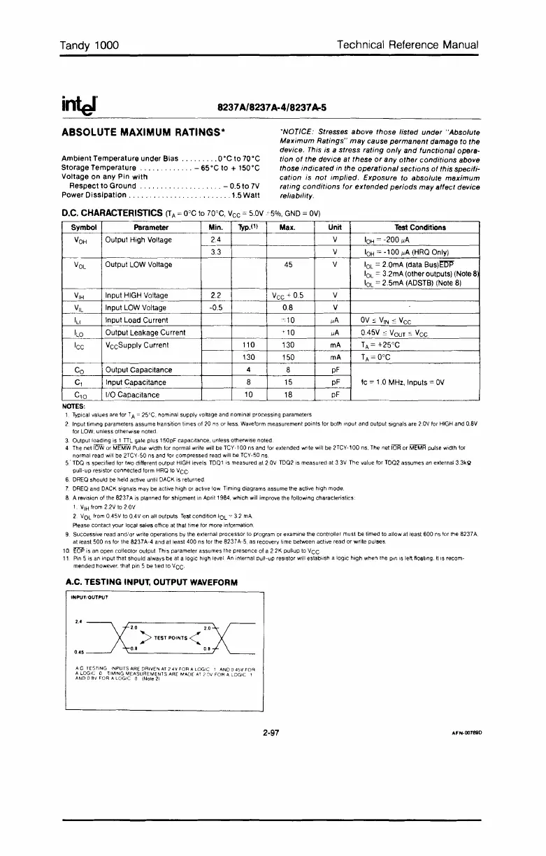
A.C. TESTING INPUT, OUTPUT WAVEFORM
,.
=x'.
>
"".,
..
,,<
"X=
0.45 0.8 0.8
AC
TESTING INPUTS ARE DRIVEN
AT
2
4'0'
FOR A LOGIC 1 AND 0
4S'o'
FOR
A LOGIC 0 TIMING
MEASUREMENTS
ARE
MADE
AT
'2
'JV
FOR A LOGIC 1
AND 0
8'0'
FOR A LOGIC 0 (NOle
21
2-97
AFN·OO789D
 Loading...