 Loading...


Do you have a question about the Tandy 1000 and is the answer not in the manual?
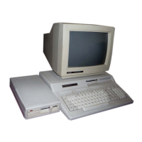
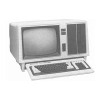
| Processor | Intel 8088 |
|---|---|
| Processor Speed | 4.77 MHz |
| RAM | 128 KB (expandable to 640 KB) |
| Operating System | MS-DOS 2.11 |
| Manufacturer | Tandy Corporation |
| Release Year | 1984 |
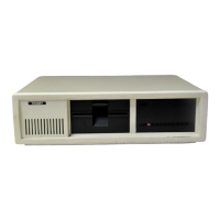
| Storage | Single or double 5.25" floppy disk drive (360 KB), optional hard drive |
| Sound | Tandy 3-voice sound |
| Ports | Parallel, Serial |
| Graphics | CGA (Color Graphics Adapter) |
| Graphics Modes | 320x200, 640x200 |