LE910Cx Hardware Design Guide
1VV0301298 Rev.40 Page 105 of 149 2023-03-16
Not Subject to NDA
It is not recommended to place a via or micro-via not covered by solder resist around the
pads in an area of 0.15 mm unless it carries the same signal as the pad itself. Micro vias
inside the pads are allowed.
Holes in pad are only allowed for blind holes and not for through holes.
Finish Layer Thickness (um) Properties
Electro-less Ni / Immersion Au 3-7 / 0.03-0.15
Good solder ability protection, high
shear force values
Table 43: Recommendations for PCB Pad Surfaces
The PCB must be able to resist the higher temperatures, which occur during the lead-
free process. This issue should be discussed with the PCB-supplier. In general, the
wettability of tin-lead solder paste on the described surface plating is better compared
to lead-free solder paste.
Solder Paste
We recommend using only “no clean” solder paste to avoid the cleaning of the modules
after assembly.
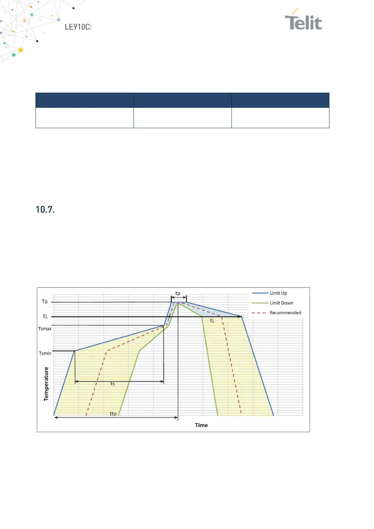
10.7.1. Solder Reflow
Figure 36 shows the recommended solder reflow profile.
Figure 36: Solder Reflow Profile
 Loading...