LE910Cx Hardware Design Guide
1VV0301298 Rev.40 Page 77 of 149 2023-03-16
Not Subject to NDA
1.8V CMOS level
Up to 50 MHz clock rate
Note: The LE910Cx module supports Master mode only and cannot
be configured as Slave mode.
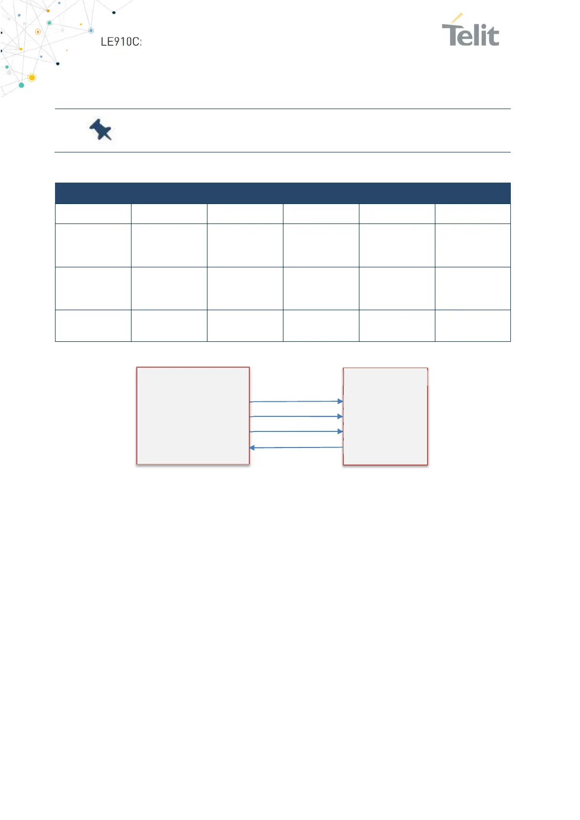
PAD Signal I/O Function Type Comment
F15 SPI_CLK O SPI clock output 1.8V
E15 SPI_MISO I SPI data Master
input Slave
output
1.8V Shared with
RX_AUX
D15 SPI_MOSI O SPI data Master
output Slave
input
1.8V Shared with
TX_AUX
H14 SPI_CS O SPI chip-select
output
1.8V
Table 30: SPI Signals
Figure 18: SPI Signal Connectivity
8.5.2. I2C - Inter-integrated Circuit
The LE910Cx supports an I2C interface on the following pins:
B11 - I2C_SCL
B10 - I2C_SDA
The I2C can also be used externally by the end customer application.
In addition, SW emulated I2C functionality can be used on GPIO pins 1-10. Any GPIO
(among GPIO 1-10) can be configured as SCL or SDA.
LE910Cx only supports I2C Master Mode.
LE910Cx
(Master)
SPI_CS
SPI_CLK
SPI_MOSI
SPI_MISO
Host (Slave)
SPI_CS
SPI_CLK
SPI_MOSI
SPI_MISO
 Loading...