LE910Cx Hardware Design Guide
1VV0301298 Rev.40 Page 88 of 149 2023-03-16
Not Subject to NDA
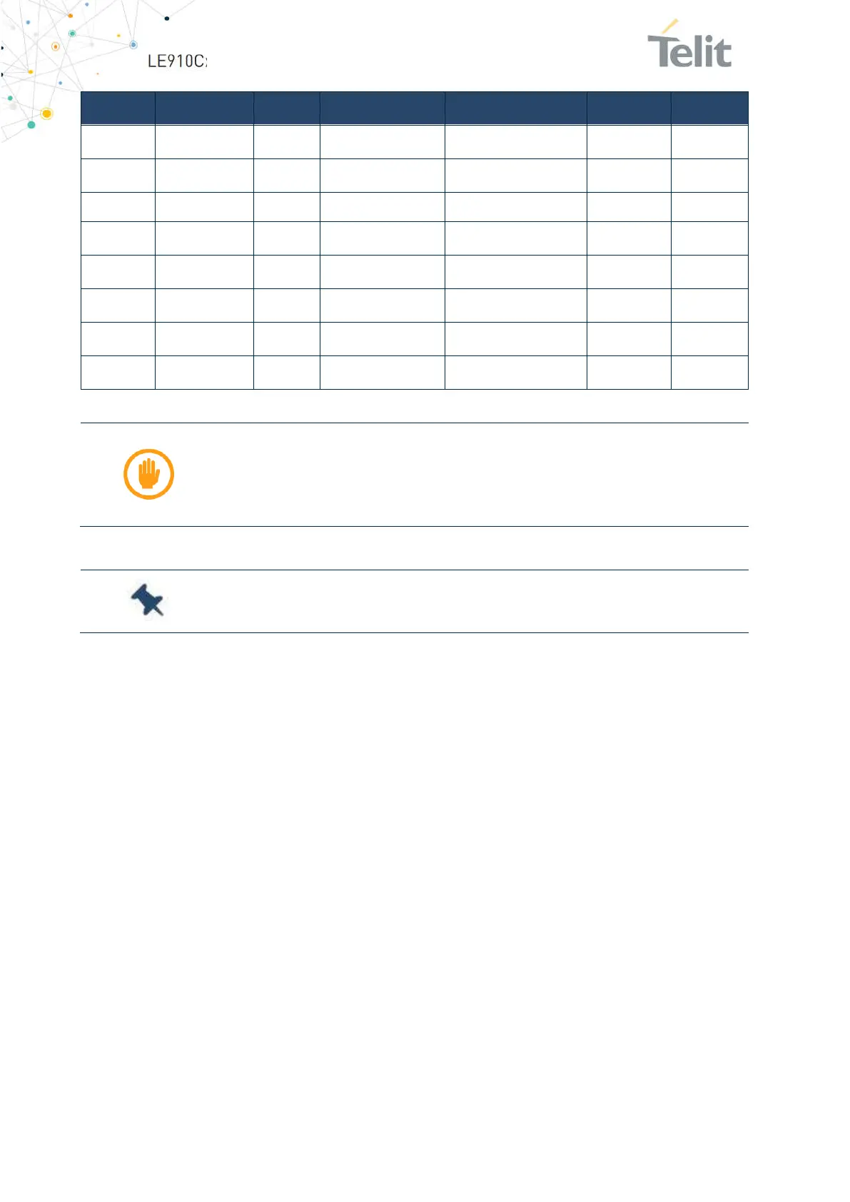
PAD Signal I/O Initial Function Alternate Function Type Note
R14 GPIO_31 I/O UART_RI Configurable GPIO CMOS 1.8V
P14 GPIO_32 I/O UART_DSR Configurable GPIO CMOS 1.8V
N14 GPIO_33 I/O UART_DCD Configurable GPIO CMOS 1.8V
M14 GPIO_34 I/O UART_DTR Configurable GPIO CMOS 1.8V
F15 GPIO_35 I/O SPI_CLK Configurable GPIO CMOS 1.8V
E15 GPIO_36 I/O SPI_MISO Configurable GPIO CMOS 1.8V
D15 GPIO_37 I/O SPI_MOSI Configurable GPIO CMOS 1.8V
H14 GPIO_11 I/O SPI_CS Configurable GPIO CMOS 1.8V
Table 38: Additional GPIOs
Warning: GPIO’s marked with (*) should not be pulled high externally
(from the carrier board) during module power on procedure. Pulling
these pads high during module power up might lead to
unwanted/non-operational boot mode.
Note: LE910Cx GPIOs 1~10 can also be used as alternate I2C function.
Refer to Section 8.5.2, I2C - Inter-integrated Circuit.
8.7.1. Using a GPIO Pad as Input
GPIO pads, when used as inputs, can be connected to a digital output of another device
and report its status, provided that this device has interface levels compatible with the
1.8V CMOS levels of the GPIO.
If the digital output of the device is connected to the GPIO input, the pad has interface
levels other than 1.8V CMOS. It can be buffered with an open collector transistor with a
10 kΩ pull-up resistor to 1.8V.
 Loading...