LE910Cx Hardware Design Guide
1VV0301298 Rev.40 Page 100 of 149 2023-03-16
Not Subject to NDA
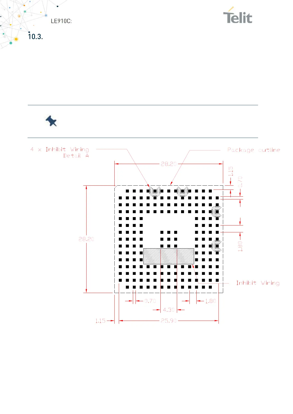
Recommended Footprint for the Application
Figure 30 and 32-1 shows the recommended footprint for the application board
(dimensions are in mm).
To facilitate the replacement of the LE910Cx module if necessary, it is suggested to
design the application board with a 1.5 mm placement inhibit area around the module.
It is also suggested, as a common rule for an SMT component, to avoid having a
mechanical part of the application board in direct contact with the module.
Note: In the customer application, the region marked as INHIBIT
WIRING in Figure 30 and 32-1 must be clear of signal wiring or
ground polygons.
Figure 30: Recommended Footprint, Copper pattern - Top View, 181 pads for LE910Cx variants except for
LE910Cx-WWX (dimensions in mm)
 Loading...