A1 A2
A3
A4
A5 A6
A7
A8 A9
B1 B2
B3
B4
B5 B6
B7
B8 B9
C1 C2
D1 D2 D4
D5 D6
D7
D8 D9
E1 E2 E4
E5 E6
E7
E8 E9
F1 F2 F4
F5 F8 F9
G1 G2 G4
G5 G8 G9
J1 J2 J4
J5 J6
J7
J8 J9
H1 H2 H4
H5 H6
H7
H8 H9
C4
C5 C6
C7
C8 C9
D3
E3
F3
G3
J3
H3
F6
G6
F7
G7
P6.0 RST/NMI
PJ.2
TEST
AVSS2 VUSB
VBUS
PU.1
PU.0
P6.2 P6.1
PJ.3
P5.3
P5.2 V18
PUR
VSSU VSSU
P6.4
P6.3
P6.6
P6.5
Reserved
Reserved Reserved
P4.4
P4.3 P4.2
P5.0 P5.1 Reserved
Reserved Reserved
P4.1
P4.0 DVCC2
P5.4 AVCC1 Reserved
Reserved Reserved DVSS2
P5.5 AVSS1 P1.3
P1.6 P3.2 P3.3
DVSS1 VCORE P1.5
P2.0 P2.2
P2.4
P2.5 P2.6
DVCC1 P1.0 P1.4
P1.7 P2.3
P2.7
P3.0 P3.1
PJ.1
PJ.0 Reserved
P4.7
P4.6 P4.5
P6.7
Reserved
Reserved
Reserved
P1.2
P1.1
Reserved
P2.1
Reserved
P3.4
MSP430F5529
,
MSP430F5528
,
MSP430F5527
,
MSP430F5526
MSP430F5525
,
MSP430F5524
,
MSP430F5522
,
MSP430F5521
MSP430F5519, MSP430F5517, MSP430F5515, MSP430F5514, MSP430F5513
SLAS590M –MARCH 2009–REVISED NOVEMBER 2015
www.ti.com
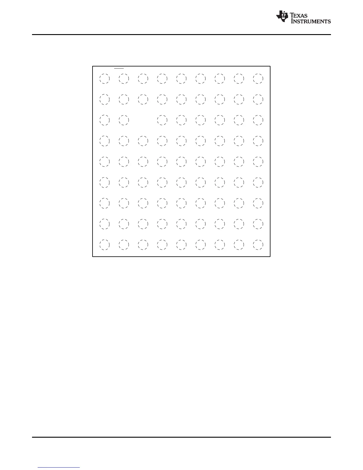
Figure 4-5 shows the pinout for the MSP430F5528, MSP430F5526, MSP430F5524, MSP430F5522,
MSP430F5514, and MSP430F5513 devices in the ZQE package.
Figure 4-5. Pin Designation – MSP430F5528IZQE, MSP430F5526IZQE, MSP430F5524IZQE,
MSP430F5522IZQE, MSP430F5514IZQE, MSP430F5513IZQE (Top View)
12 Terminal Configuration and Functions Copyright © 2009–2015, Texas Instruments Incorporated
Submit Documentation Feedback
Product Folder Links: MSP430F5529 MSP430F5528 MSP430F5527 MSP430F5526 MSP430F5525 MSP430F5524
MSP430F5522 MSP430F5521 MSP430F5519 MSP430F5517 MSP430F5515 MSP430F5514 MSP430F5513