Copyright © 2009–2017, Texas Instruments Incorporated Peripheral Information and Electrical Specifications
Submit Documentation Feedback
Product Folder Links: TMS320C6748
167
TMS320C6748
www.ti.com
SPRS590G –JUNE 2009–REVISED JANUARY 2017
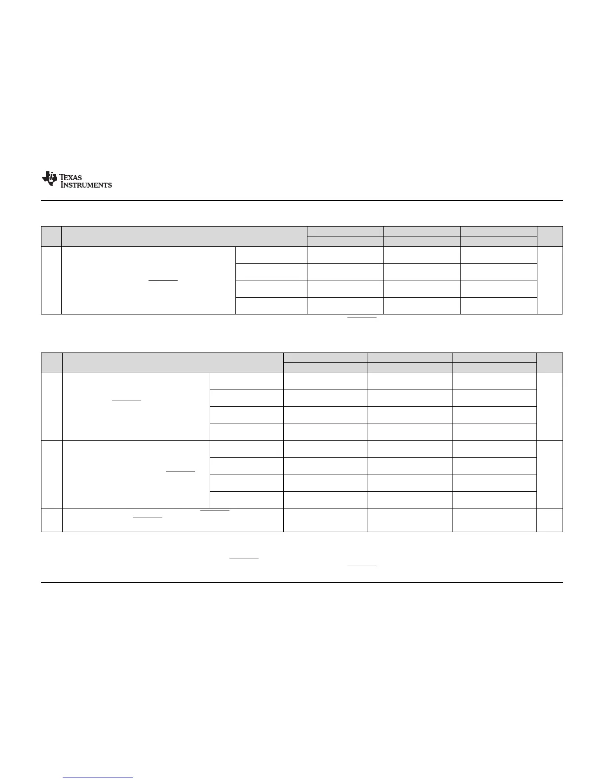
Table 6-71. Additional SPI0 Master Timings, 4-Pin Chip Select Option
(1)(2)(3)
(continued)
NO. PARAMETER
1.3V, 1.2V 1.1V 1.0V
UNIT
MIN MAX MIN MAX MIN MAX
(6) Except for modes when SPIDAT1.CSHOLD is enabled and there is additional data to transmit. In this case, SPI0_SCS will remain asserted.
(7) This delay can be increased under software control by the register bit field SPIDELAY.T2CDELAY[4:0].
20 t
d(SPC_SCS)M
Delay from final SPI0_CLK edge to master
deasserting SPI0_SCS
(6) (7)
Polarity = 0, Phase = 0,
from SPI0_CLK falling
0.5M+P-1 0.5M+P-2 0.5M+P-3
ns
Polarity = 0, Phase = 1,
from SPI0_CLK falling
P-1 P-2 P-3
Polarity = 1, Phase = 0,
from SPI0_CLK rising
0.5M+P-1 0.5M+P-2 0.5M+P-3
Polarity = 1, Phase = 1,
from SPI0_CLK rising
P-1 P-2 P-3
(1) These parameters are in addition to the general timings for SPI master modes (Table 6-69).
(2) P = SYSCLK2 period; M = t
c(SPC)M
(SPI master bit clock period)
(3) Figure shows only Polarity = 0, Phase = 0 as an example. Table gives parameters for all four master clocking modes.
(4) In the case where the master SPI is ready with new data before SPI0_ENA deassertion.
(5) Except for modes when SPIDAT1.CSHOLD is enabled and there is additional data to transmit. In this case, SPI0_SCS will remain asserted.
(6) This delay can be increased under software control by the register bit field SPIDELAY.T2CDELAY[4:0].
Table 6-72. Additional SPI0 Master Timings, 5-Pin Option
(1)(2)(3)
NO. PARAMETER
1.3V, 1.2V 1.1V 1.0V
UNIT
MIN MAX MIN MAX MIN MAX
18 t
d(SPC_ENA)M
Max delay for slave to deassert
SPI0_ENA after final SPI0_CLK
edge to ensure master does not
begin the next transfer.
(4)
Polarity = 0, Phase = 0,
from SPI0_CLK falling
0.5M+P+5 0.5M+P+5 0.5M+P+6
ns
Polarity = 0, Phase = 1,
from SPI0_CLK falling
P+5 P+5 P+6
Polarity = 1, Phase = 0,
from SPI0_CLK rising
0.5M+P+5 0.5M+P+5 0.5M+P+6
Polarity = 1, Phase = 1,
from SPI0_CLK rising
P+5 P+5 P+6
20 t
d(SPC_SCS)M
Delay from final SPI0_CLK edge to
master deasserting SPI0_SCS
(5)
(6)
Polarity = 0, Phase = 0,
from SPI0_CLK falling
0.5M+P-2 0.5M+P-2 0.5M+P-3
ns
Polarity = 0, Phase = 1,
from SPI0_CLK falling
P-2 P-2 P-3
Polarity = 1, Phase = 0,
from SPI0_CLK rising
0.5M+P-2 0.5M+P-2 0.5M+P-3
Polarity = 1, Phase = 1,
from SPI0_CLK rising
P-2 P-2 P-3
21 t
d(SCSL_ENAL)M
Max delay for slave SPI to drive SPI0_ENA valid after master
asserts SPI0_SCS to delay the master from beginning the
next transfer,
C2TDELAY+P C2TDELAY+P C2TDELAY+P ns
 Loading...


