Note
After the MCU_TO_WARM sequence the MCU is responsible for managing the EN_DRV and
recovery counter. At the end of the sequence the 'FORCE_EN_DRV_LOW' bit is cleared so that
the MCU can set the ENABLE_DRV bit.
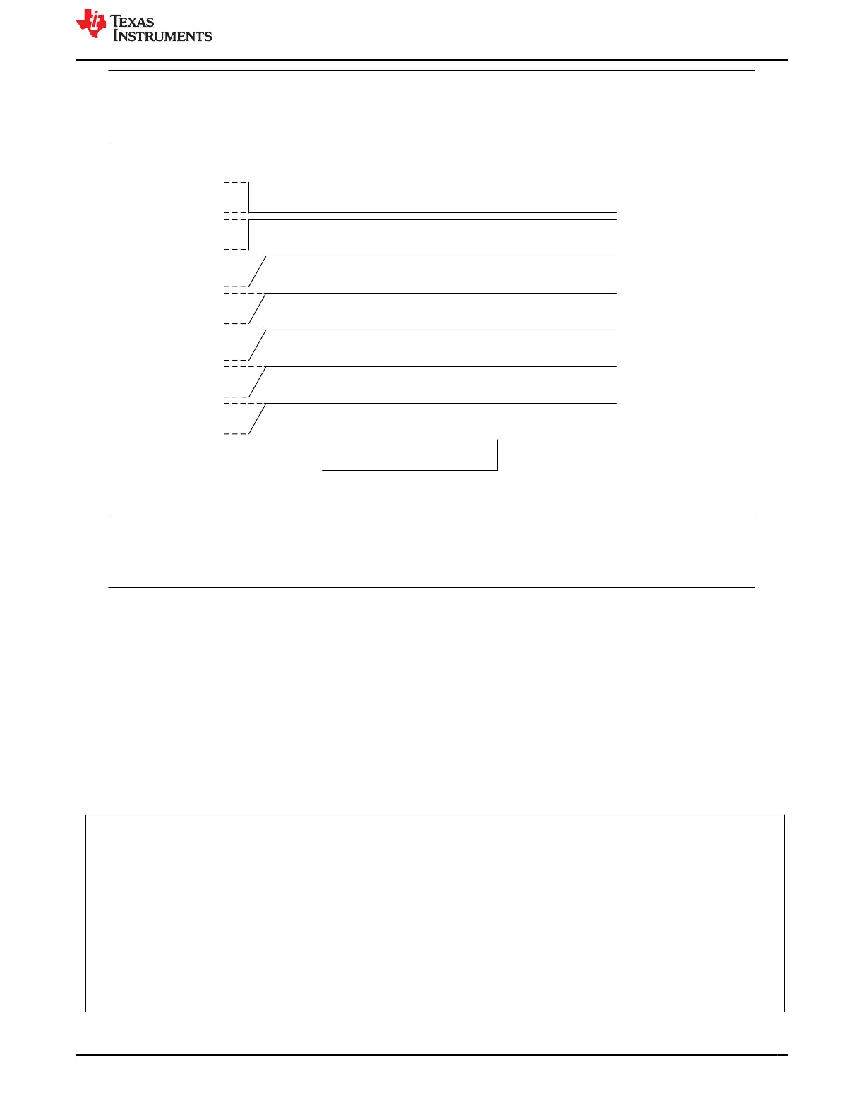
Resource PMIC Delay Diagram Total Delay Rail Name
GPIO9
TPS65941120-Q1
(Leo A)
0 us EN_MCU3V3_VIO
LDO2
TPS65941120-Q1
(Leo A)
0 us
VDD_MCU_
GPIORET_3V3
LDO4
TPS65941120-Q1
(Leo A)
0 us VDA_MCU_1V8
LDO3
TPS65941120-Q1
(Leo A)
0 us VDD_MCUIO_1V8
BUCK5
TPS65941120-Q1
(Leo A)
0 us VDD_MCU_0V85
LDO1
TPS65941120-Q1
(Leo A)
0 us VDD_MCU_WK_0V8
nRSTOUT
TPS65941120-Q1
(Leo A)
2000 us H_MCU_PORz
nRSTOUT
TPS65941120-Q1
(Leo A)
0 us H_MCU_PORz
Figure 6-8. MCU_TO_WARM Sequence
Note
The regulator transitions do not represent enabling of the regulators but the time at which the voltages
are restored to their default values. Since this sequence originates from the MCU_ONLY state these
regulators are on.
6.3.7 TO_MCU
The TO_MCU sequence first turns off rails and GPIOs which are assigned to the SOC power group. The
sequence enables the MCU rails, in the event that they are not already active (when transitioning from
STANDBY to MCU_ONLY for example). This sequence can be changed based off the value stored in the
I2C_6 and I2C_7 register bit of all PMICs. The I2C_6 and I2C_7 settings must be the same in each PMIC before
triggering the sequence. If the I2C_7 bits are low, then EN_DDR_VDD1 and VDD_DDR_1V1 are disabled; If
the I2C_6 bits are low, then VDD_GPIORET_3V3 and VDD_WK_0V8 are disabled as seen in Figure 6-10. If
the I2C_7 bits are high, then EN_DDR_VDD1 and VDD_DDR_1V1 are enabled; If the I2C_6 bits are high, then
VDD_GPIORET_3V3 and VDD_WK_0V8 are enabled as seen in Figure 6-9.
The first instructions of the TO_MCU sequence perform writes to the MISC_CTRL and ENABLE_DRV_STAT
registers.
// TPS65941120
// Set AMUXOUT_EN, CLKMON_EN
// Clear LPM_EN, NRSTOUT_SOC
REG_WRITE_MASK_IMM ADDR=0x81 DATA=0x18 MASK=0xE1
// Clear SPMI_LP_EN
REG_WRITE_MASK_IMM ADDR=0x82 DATA=0x00 MASK=0xEF
// TPS65941421
// Set AMUXOUT_EN, CLKMON_EN
// Clear LPM_EN
REG_WRITE_MASK_IMM ADDR=0x81 DATA=0x18 MASK=0xE3
// Clear SPMI_LP_EN
REG_WRITE_MASK_IMM ADDR=0x82 DATA=0x00 MASK=0xEF
// LP876411B5
// Set CLKMON_EN
// Clear LPM_EN
www.ti.com Pre-Configurable Finite State Machine (PFSM) Settings
SLVUCJ9 – FEBRUARY 2023
Submit Document Feedback
TPS65941120-Q1, TPS65941421-Q1 and LP876411B5-Q1 PMIC User Guide
for J721S2, PDN-0A
43
Copyright © 2023 Texas Instruments Incorporated
 Loading...


