300/400TS and 300/400S 11 ADVANCED TROUBLESHOOTING
11 – 14
5.4 Verification of the Gas Valve,
SOL1, Drive Circuitry
CAUTION
Before performing any portion of the procedure
below, make certain the unit is placed in the initial
set up condition as described in section 11.4.1
"Preparation".
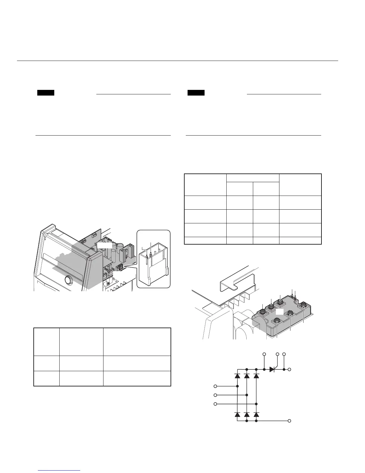
1) Verify the voltage between t
he PIN 3 (Positive
[+]) and PIN 4 (Negative [-]) of connector CN11
on PCB3 (WK-5548) while you press the torch
switch while in TIG Mode. (The capacity of the
voltmeter should be more than 50VDC.) The
location of connector CN11 of PCB3 (WK-
5548) is indicated in Figure 11-13. When you
measure the above voltage, do not remove the
connector. Conduct the measurement while
the connector plug and receptacle are still con-
nected.
Figure 11-13: Verification of the SOL1
2) Using the measurement taken above, follow
the chart below for possible failure modes.
Table11-4: Verification of the SOL1
3) When verifying the voltage, confirm that the AC
input voltage remain within the operating range
of the unit.
(The AC input does not drop below 180VAC).
5.5 Verification of the primary
Diode (D1)
CAUTION
Before performing any portion of the procedure
below, make certain the unit is placed in the initial
set up condition as described in section 11.4.1
"Preparation".
1) Verify the characteristic of the primary diode,
D1, using a diode tester.
2) Refer
to Table 11-5 and Figure 11-14 for
the checkpoints on D1.
Table11-5: Tester checkpoints in D1
Figure11-14: Tester checkpoints for D
1 showing
the interconnection diagrams
Voltage
measurement.
(PIN 3-PIN 4 of
CN11 on PCB3)
Remedy
Case 1 Below DC 18V
Replace PCB1.
Refer to section 12.3.1
Case 2
DC 18 ∼ 25V
Replace SOL1.
Refer to section 12.3.22
PCB3
CN11
pin 3
pin 4
COMPONENT
TESTED
TERMINALS
ACCEPTABLE
VALUE
Positive
lead
Negative
lead
Diode of D1
3, 4, 5
0
0
3, 4, 5
0.3 to 0.5V
Open
Diode of D1
3, 4, 5
2
2
3, 4, 5
Open
0.3 to 0.5V
Thyristor of D1
0
1
1
0
Open
Open
Gate of D1 6 7 52 +3, ±3ohm
D1
5
6
7
4
3
2
1
0
067
1
2
5
4
3



 To Next Page