ML505/ML506/ML507 Evaluation Platform www.xilinx.com 39
UG347 (v3.1.1) October 7, 2009
Detailed Description
R
The JTAG debug port supports the four required JTAG signals: TCK, TMS, TDI, and TDO.
It also implements the optional TRST signal. The frequency of the JTAG clock signal can
range from 0 MHz (DC) to one-half of the processor clock frequency. The JTAG debug port
logic is reset at the same time the system is reset, using TRST. When TRST is asserted, the
JTAG TAP controller returns to the test-logic reset state.
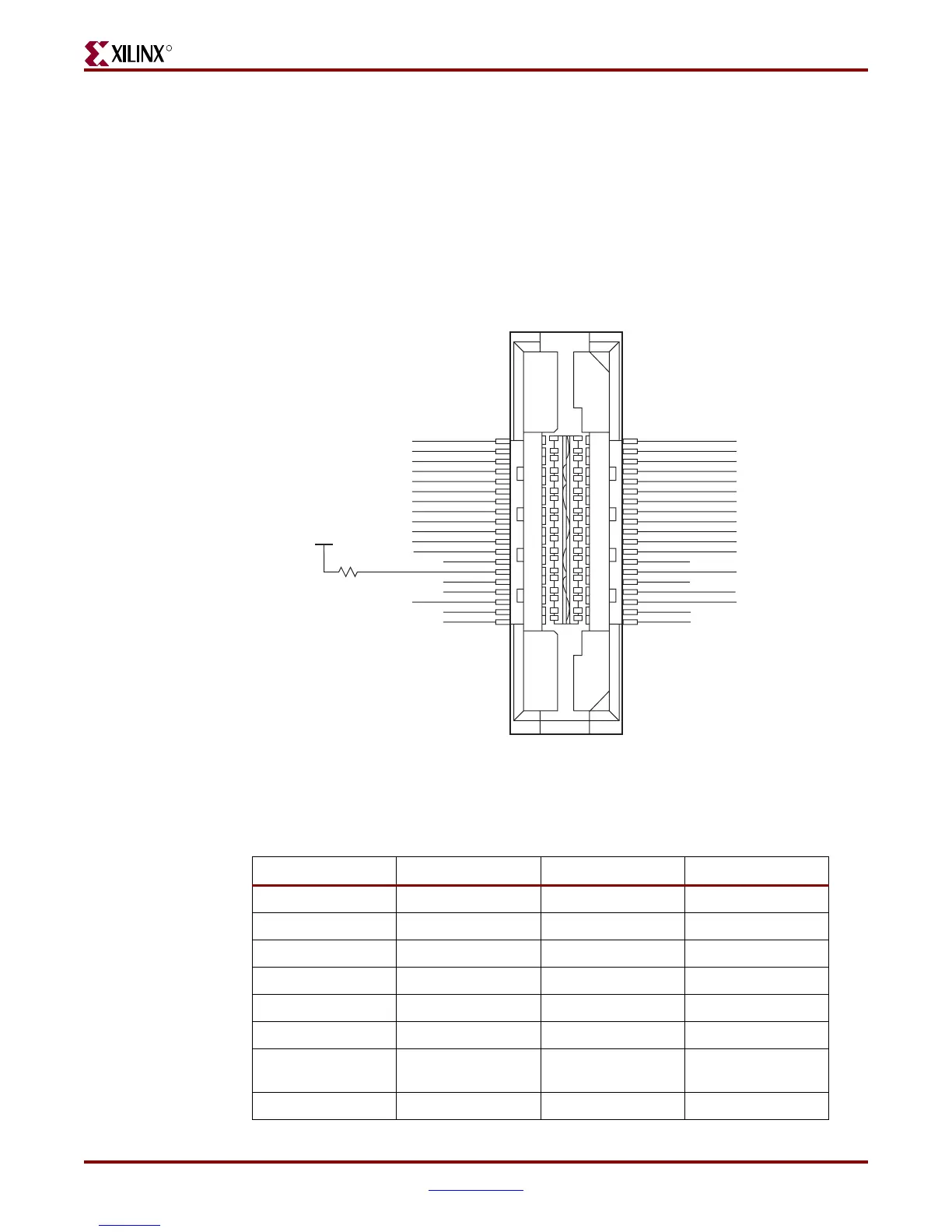
Figure 1-7 shows a 38-pin Mictor connector that combines the CPU Trace and the CPU
Debug interfaces for high-speed, controlled-impedance signaling.
Note:
MICTOR_* pins are only available on the ML507 board. These pins are not connected on the
ML505 and ML506 boards.
Table 1-21 shows the CPU trace/debug connections from P22 to the FPGA and BDM.
Figure 1-7: Combined Trace/Debug Connector Pinout
Table 1-21: CPU Trace/Debug Connection to FPGA
Pin Name
(1)
FPGA Pin (U1) Mictor Pin (P22) BDM Pin (J51)
-NC1
-NC2
-3
-NC4
MICTOR_5 A24 5
TRC_CLK AD9 6
PC4_HALT_B
(CPU_HALT_N)
W9 7 11
-NC8
37
35
33
31
29
27
25
23
21
19
17
15
13
11
9
7
5
3
1
CPU_TRST
FPGA_CS0_B
CPU_TMS
CPU_TCK
NC
NC
NC
NCNC
NC
NC
NC
NC
MICTOR_16
MICTOR_29
MICTOR_27
MICTOR_25
MICTOR_23
MICTOR_37
MICTOR_35
MICTOR_33
MICTOR_31
CPU_TDO
PC4_HALT_B
MICTOR_5
TRC_TS6
TRC_TS5
TRC_TS4
TRC_TS3
TRC_TS1E
TRC_TS2E
TRC_TS2O
TRC_TS1O
MICTOR_20
MICTOR_22
MICTOR_18
TRC_CLK
TRC_VSENSE
38
36
34
32
30
28
26
24
22
20
18
16
14
12
10
8
6
4
2
Mictor 38 (P22)
2.5V
UG347_06_011008
GND, G1, G2, G3, G4, G5
Downloaded from Elcodis.com electronic components distributor