VCU118 Board User Guide 35
UG1224 (v1.0) December 15, 2016
www.xilinx.com
Chapter 3: Board Component Descriptions
The VCU118 RLD3 72-bit memory component interface adheres to the constraints
guidelines documented in the RLD3 Design Guidelines section of UltraScale
Architecture-Based FPGAs Memory IP LogiCORE IP Product Guide (PG150) [Ref 4]. The
VCU118 RLD3 memory component interface is a 40Ω impedance implementation. For more
information on the internal VREF, see the "Supply Voltages for the SelectIO Pins", “V
REF
”,
and “Internal V
REF
” sections in UltraScale Architecture SelectIO Resources (UG571) [Ref 3].
For more details about the Micron RLD3 component memory, see the Micron
MT44K32M36RB-083E Data Sheet [Ref 18].
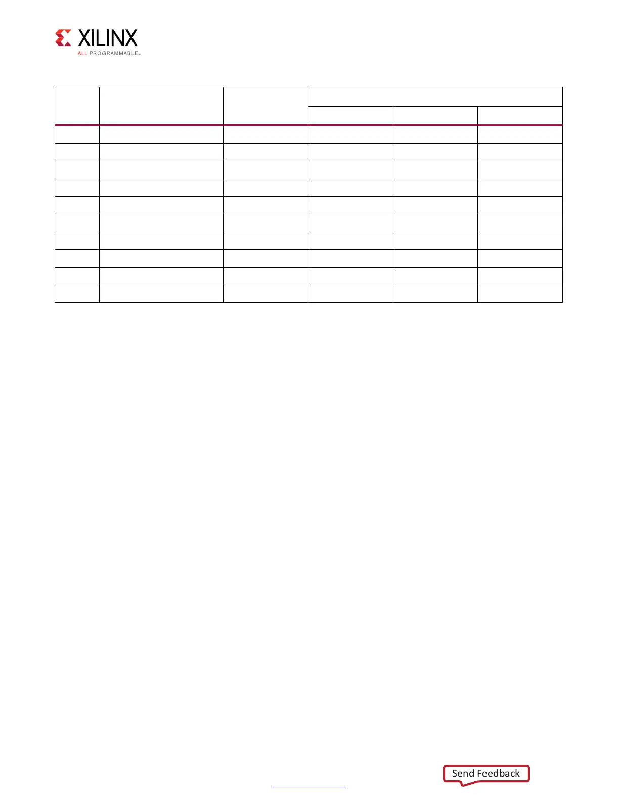
L29 RLD3_C3_72B_RESET_B SSTL12 A13 RESET_B U141-U142
N29 RLD3_C3_72B_CS_B SSTL12 E12 CS_B U141-U142
K31 RLD3_C3_72B_DK0_P DIFF_SSTL12 D7 DK0 U141
J31 RLD3_C3_72B_DK0_N DIFF_SSTL12 C7 DK0_B U141
K32 RLD3_C3_72B_DK1_P DIFF_SSTL12 K7 DK1 U141
J32 RLD3_C3_72B_DK1_N DIFF_SSTL12 L7 DK1_B U141
J29 RLD3_C3_72B_DK2_P DIFF_SSTL12 D7 DK0 U142
J30 RLD3_C3_72B_DK2_N DIFF_SSTL12 C7 DK0_B U142
H33 RLD3_C3_72B_DK3_P DIFF_SSTL12 K7 DK1 U142
G33 RLD3_C3_72B_DK3_N DIFF_SSTL12 L7 DK1_B U142
Table 3-4: RLD3 Memory 72-bit I/F to FPGA U1 Banks 46, 47, and 48 (Cont’d)
FPGA
(U1) Pin
Schematic Net Name I/O Standard
Component Memory
Pin # Pin Name Ref. Des.