PCE-5126 User Manual 6
1.5 Board Layout: Jumper and Connector
Locations
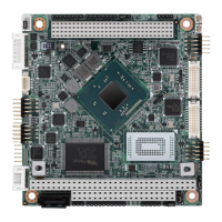
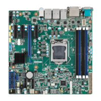
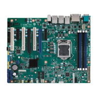
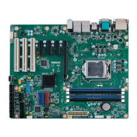
Figure 1.1 Jumper and connector locations
CPU1 CPU Socket
DIMMA1 Memory connector channel A
DIMMB1 Memory connector channel B
GPIO1 GPIO pin header (SMD pitch-2.0 mm)
LPC1 COM port module expansion pin-header
Table 1.2: Connector list
Label Function