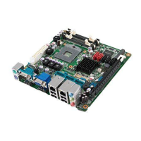
PCE-5126 User Manual 84
C.1 Supported GPIO Register
Below are the detailed descriptions of the GPIO addresses and programming sam-
ple.
C.2 GPIO registers
C.3 GPIO example program-1
------------------------------------------------
Enter the extended function mode, interruptible double-write
------------------------------------------------
MOV DX,2EH
MOV AL,87H
OUT DX,AL
OUT DX,AL
---------------------------------------------------------------
Configure logical device, configuration register CRE0,CRE1,CRE2
---------------------------------------------------------------
MOV DX,2EH
MOV AL,09H
OUT DX,AC
DEC DX
MOV AL,30H
OUT DX,AL
INC DX
IN AL,DX
OR AL,10000000B
DEC DX
MOV AL,07H
OUT DX,AL
Bank Offset Description
09h 30h Write 1 to bit 7 to enable GPIO
07h E0h
GPIO I/O Register
When set to a '1', respective GPIO port is pro-
grammed as an input port.
When set to a '0', respective GPIO port is pro-
grammed as an output port.
07h E1h
GPIO Data Redister
If a port is programmed to be an output port, then
its respective bit can be read/written.
If a port is programmed to be an input port, then its
respective bit can only be read.
07h E2h
GPIO Inversion Register
When set to a '1', the incoming/outgoing port value
is inverted.
When set to a '0', the incoming/outgoing port value
is the same as in data register.