134
5
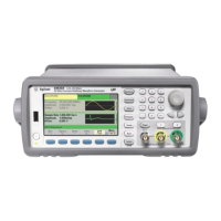
The signal is applied to the output amplifier. The DC offset is summed at
the output amplifier. A post amplifier -23.87 dB attenuator is available
for low level signals. The table below show the attenuators used to create
the desired output signal amplitude.
The output relay when enabled provides the waveform to the front panel
BNC connector. Additionally, this relay, when disabled, routes the signal
to the Modulation ADC for internal self-test and calibration routines.
The output relay is controlled by the FPGA. Two circuits provide
overvoltage and over current protection. The protection circuits
primarily provide protection against injected voltages or currents from
an external circuit. The waveform generator is capable of sourcing very
low output impedances.
Output Range
DC Offset < 320 mV
-7.96 dB -15.91 dB -23.87 dB
-23.87 dB
(post)
10 V
PP
- 3.6 V
PP
Out Out Out Out
4 V
PP
- 1.44 V
PP
In Out Out Out
1.6 V
PP
- 576 mV
PP
Out In Out Out
640 mV
PP
- 230 mV
PP
Out Out Out In
256 mV
PP
- 92 mV
PP
In Out Out In
102.4 mV
PP
- 36.86 mV
PP
Out In Out In
40.96 mV
PP
- 14.75 mV
PP
Out Out In In
16.38 mV
PP
- 5.90 mV
PP
In Out In In
6.55 mV
PP
- 2.36 mV
PP
Out In In In
2.62 mV
PP
- 1.00 mV
PP
In In In In
Output Range
(DC Offset >
320 mV)
-7.96 dB -15.91 dB -23.87 dB
-23.87 dB
(post)
9.36 V
PP
- 3.6 V
PP
Out Out Out Out
4 V
PP
- 1.44 V
PP
In Out Out Out
1.6 V
PP
- 576 mV
PP
Out In Out Out
640 mV
PP
- 230 mV
PP
Out Out In Out
256 mV
PP
- 92 mV
PP
In Out In Out
102.4 mV
PP
- 36.86 mV
PP
Out In In Out
40.96 mV
PP
- 1.00 mV
PP
In In In Out
 Loading...