Agilent N5181A/82A MXG Signal Generators User’s Guide 13
Signal Generator Overview
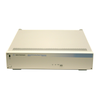
Rear Panel Overview
PAT TRIG IN
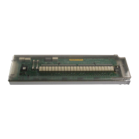
DIGITAL BUS I/O
This is a proprietary bus used by Agilent Technologies signal creation software. This connector is not
operational for general purpose use. Signals are present only when a signal creation software option
is installed (for details, refer to http://www.agilent.com/find/signalcreation).
AUX I/O
Connector female BNC Impedance: nominally 50Ω
Signal A TTL/CMOS low to TTL/CMOS high, or TTL/CMOS high to TTL/CMOS low edge trigger.
The input to this connector triggers the internal digital modulation pattern generator to start a
single pattern output or to stop and re- synchronize a pattern that is being continuously output.
To synchronize the trigger with the data bit clock, the trigger edge is latched, then sampled
during the falling edge of the internal data bit clock.
This is the external trigger for all ARB waveform generator triggers.
Minimum Trigger Input Pulse Width (high or low) = 100 ns
Minimum Trigger Delay (trigger edge to first bit of frame) = 1.5 to 2.5 bit clock periods
Damage Levels > +8 and < −4V
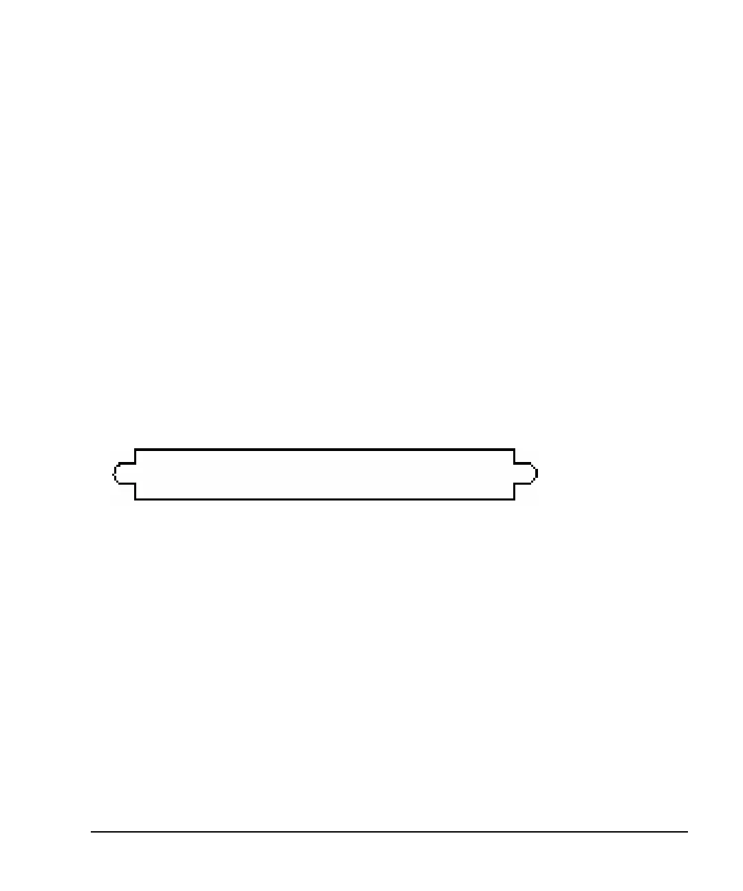
View looking into rear panel female 50-pin connector
25
1
2650
Pin 1 = Event 1
Pin 2 = Event 2
Pin 3 = Event 3
Pin 4 = Event 4
Pin 5 = Sample Rate Clock Ou
Pin 6 = Patt Trig In 2
Pins 7–25 = Reserved*
Pins 26–50 = Ground
*Future Capability
vent 1, 2, 3, and 4 (pins 1 − 4)
pulse that can be used to trigger the start of a data pattern, frame, or timeslot.
djustable to ± one timeslot; resolution = one bit
arkers
ach Arb-based waveform point has a marker on/off condition associated with it.
arker level = +3.3V CMOS high (positive polarity selected); –3.3V CMOS low (negative polarity selected).
utput on these pins occurs whenever the corresponding marker is on in an Arb-based waveform (see “Using Waveform Markers” on
age 82).
att Trig In 2 (pin 6)
TTL/CMOS low to TTL/CMOS high, or TTL/CMOS high to TTL/CMOS low edge trigger.
he input to this connector triggers the internal digital modulation pattern generator to start a single pattern output or to stop and
e-synchronize a pattern that is being continuously output.
o synchronize the trigger with the data bit clock, the trigger edge is latched, then sampled during the falling edge of the internal data bit
lock.
his is an external trigger for all ARB waveform generator triggers. Minimum pulse width = 100 ns. Damage levels: > +5.5 and < −0.5V.
ample Rate Clock Out (pin 5)
his output is used with an internal baseband generator. This pin relays a CMOS bit clock signal for synchronizing serial data.
amage levels: > +5.5 and < −0.5V.