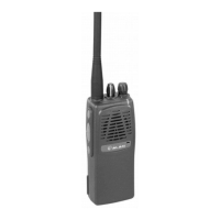
HP406 Service Manual
Page 5 of 12
The synthesizer is tuned in 5.00 KHz or 6.25 KHz step.
2.3.c Synthesizer
The frequency synthesizer is a large scale monolithic synthesizer integrated circuit
Q429
.
The synthesizer IC contains a dual modular prescaler, programmable divide-by-N counter, prescaler control
(swallow) counter, reference oscillator, reference divider, phase detector, charge pump and lock detector.
Also, included in
Q429
are shift registers and control circuits for frequency controls and general device control.
RF output from the active VCO is AC coupled to the synthesizer
Q429
prescaler input at Pin
8
. The divide-by-N
counter chain in
Q429
, consisting of the dual-modulus prescaler, swallow counter and programmable counter,
divides the VCO signal down to a frequency very close to 5.00 KHz or 6.25 KHz which is applied to the phase
detector. The phase comparator compares the edges of this of this signal with that of the 5.00 KHz or 6.25 KHz
reference signal from the reference divider and drives the external charge pump (
Q425
and
Q426
).
The synthesizer unlock detector circuit prevents the operation of the transmitter, when the phase lock loop (PLL)
is unlocked. The following discussion assumes the unit has been placed in the transmit mode.
Q429
lock
detector Pin
7
goes high when the PLL is locked. This high level is applied to Pin
21
of the microprocessor
Q17
.
A software timing routing brings the
RX/TX
line low (Pin
29
of
Q17
), feeding this signal through the switch/buffer
Q15
. With the
RX/TX
line low,
Q223A
is cut off and
Q223B
is biases on passing
+5VTX
to
Q431B,
it biases on
Q430
to pass switched
TX B+
to the transmitter amplifier string which enables transmission.
When the PLL become unlocked, the lock detector at
Q429
Pin7 will begin pulsing low. A RC
circuit converts
pulsing low to a low level for the microprocessor. The microprocessor then changes the RX/TX line to a high,
thus signalling the other transistor switches to drive
Q430
into cutoff which disable transmission. Therefore, the
transmitter remains disabled while the loop remains out of lock.
2.3.d Loop Filter
The Loop Filter, a passive lead-lag filter consisting of
R461-R464
and
C493-C495
, integrates the charge pump
output to produce the DC turning voltage for the VCO. One parasitic pole, consisting of
R461
/
C493
and RF
chokes
L928
/
L929
, prevent modulation of the VCOs by the 5.00 KHz or 6.25 KHz reference energy remaining at
the output of the loop filter. Direct FM is obtained for modulating frequencies outside the PLL bandwidth by
applying the CTCSS/DCS signals and the pre-emphasized, limited microphone audio to the VCO modulation
circuit.
The modulation circuit consists of
R952
,
Q921
and
C987
.
2.4 Transmitter
2.4.a RF Power Amplifier
After the PTT is pressed, the
+5VTX
line switches to approximately 5V.
Q919
is turned on enabling transmit
VCO.
The VCO buffer, pre-driver, driver and power amplifier are biased on by
Q430
, which is biased on by the
+5VTX
line switching to 5V. RF output from the transmit VCO(
Q916
) is applied to the VCO output buffer
Q915
.
Output from
Q415
feeds the pre-driver amplifier
Q413
. The output signal from
Q413
feeds the driver amplifier
Q412
, whose output from the driver stage feeds the final RF power amplifier
Q407
to produce the rated output
power of 2 watts. The output of the final is applied to a low-pass filter(
C451
,
C452
and
L413
) and then to the
transmit/receive switch
Q402
. RF power is then fed to the antenna via the output low-pass filter consisting of
C401
,
C402
,
C404-C405
,
C407-C408
,
L401
, and
L402
.
2.4.b Antenna Switching
Switching of the antenna between the transmitter and the receiver is accomplished by the antenna
transmit/receive switch consisting of diodes
Q401
and
Q402
in conjunction with
C410
and
R402
. In the transmit
mode, switched
TX B+
is applied through
R420
and RF choke
L414
,hard forward biasing the two diodes on.
Q402
thus permits the flow of RF power from output of the low-pass filter fed by the output amplifier to the output
low-pass filter.
Q401
shorts the receiver input to
C410
, which is AC coupled to ground.
L403
,
C409
,
C410
and
R402
then function as a lumped constant quarter-wave transmission line, thus presenting a high impedance to
the RF output path, effectively isolating the receiver input and transmitter output sections.