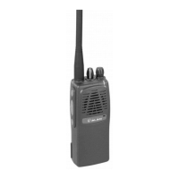
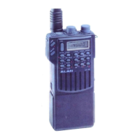
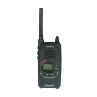
HP106 Service Manual
Page 6 of 12
2.4.c Power control
Output power is controlled via the dual Op-Amp (Q408) , which is used as a differential amplifier and comparator.
Current is sensed by the voltage drop across R421 and R422. This voltage is compared to the one set by the 2-
watt Adjustment RV401. The power output is then reduced or increased by varying the Q410's output voltage
applied to the power amplifier Q407's pin 2.
2.4.d Transmitter Audio Circuits
The transmitter audio circuits consist of the audio processing circuits, the CTCSS circuits and the DCS circuits.
2.4.e Audio Processing
Transmit speed audio is providing by either the internal electric microphone N101 or the external microphone. The
microphone audio is applied to MIC MUTE SW Q235, and Lo-pass filter Q214A, Q214B. The audio is pre -
emphasized by 6dB per octave by C236 and R284, and then signal amplification. The gain is such that when a
signal greater than 20 dB.
Limiting the peak-to-peak output. Under these conditions, the MOD. ADJ. Pot RV201 configured as a four-pole
active low-pass filter. The resulting signal is then limited when respect to side band splatter, and has an 18 dB per
octave roll-off above 3 KHz.
The audio is then applied through the 25 KHz/12.5 KHz channel spacing SW Q215 to transmit VCO. By varying
the voltage on the varactor diode Q921 at an audio rate. The resonant frequency of VCO is varied. The result is
an oscillator output that is frequency -modulated at the audio frequency.
2.5 Receiver
2.5.a Receiver Front End
In the receive mode, the RF signal enters thorough the antenna, then through the low-pass filter C401, C403,
C405-C409 and L401-L403. The diodes Q401 and Q402 are biased off so that the output of the low-pass filter is
coupled (C411) to the first band-pass filter C412-C415, C417-C420, L404-L407 and to the Front End RF overload
protection diode pair Q403. The signal from the band-pass filter is applied to the input of the RF amplifier Q404.
The output of the RF amplifier feeds the input to three more stages of band-pass filters consisting of C424-C431,
and L408-L410. The output from the band-pass filter is applied to the mixer’s Q405/L411.
2.5.b Local Oscillator (LO)
The Receive VCO (C482-C485, CV401, L426-L427, Q422-Q424 and R453-R454) provides the LO signal. The
VCO is running at 45.1 MHz above the desired receive frequency and is applied to output Buffer Q415/Q414. The
output of the buffer through the low-pass filter C433-C435, L432-L433 and applied to the mixer Q405/L411/L412.
2.5.c Mixer
The mixer is a DBM type (L411,Q405,L412). The mixer LO frequency is 45.1 MHz below the desired receiver
frequency.
When the receiver frequency is present, the mixer output will be a 45.1MHz signal. The mixer output is peaked for
45.1MHz at L434, C437 and R413, and the signal is filtered by crystal filter F401A and F401B and amplified by
Q406 before being applied to the input of the IF IC IC6.
Inside IC6, the 45.1MHz IF signal becomes the input to a second mixer with a LO frequency of 44.645 MHz set by
X201. The 455 KHz ceramic filter F201 or F202 filters the second mixer’s output which is the second IF signal.
The mixer’s output is then fed to the internal limiting amplifier and then on to the FM decoder.
2.5.d FM Detector and Squelch
The FM detector output is used for squelch, decoding tones and audio output. The setting of the squelch
adjustment potentiometer RV204 (for 25 KHz channel spacing) and RV205 (for 12.5 KHz channel spacing) sets
the input to the squelch amplifier.
The squelch amplifier is internal to IC6 and its output is fed to an internal rectifier and squelch detector.