Clock pin assignment:
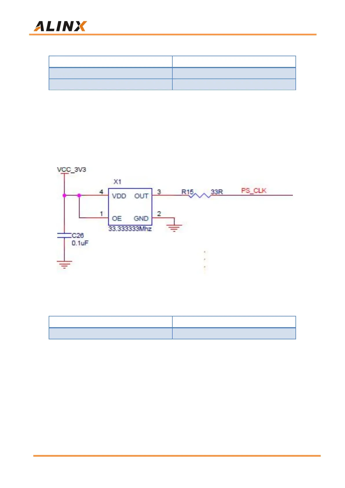
PS System Clock Source
The X1 crystal on the core board provides a 33.333MHz clock input for the
PS part. The clock input is connected to the PS_REF_CLK_503 pin of
BANK503 of the ZYNQ chip. The schematic diagram is shown in Figure 2-6-3:
Figure 2-6-3: Active Crystal in PS part
Clock pin assignment:
PL System Clock Source
The core board provides a differential 200MHz PL system clock source for
the reference clock of the DDR4 controller. The crystal oscillator output is
connected to the global clock (MRCC) of PL BANK64. This global clock can be
used to drive the DDR4 controller and user logic circuits in the FPGA. The
schematic diagram of this clock source is shown in Figure 2-6-4